
Device and process for preparing silicon carbide by PVT method

A technology of silicon carbide and carbide, which is applied in the field of PVT preparation of silicon carbide device and preparation process, can solve the problems of micropipes, carbon-wrapped growth defects, etching, etc., to ensure doping stability and resistivity distribution uniformity , reduce cost and prolong service life

Pending Publication Date: 2022-07-01
北京清研半导科技有限公司
View PDF2 Cites 0 Cited by
  • Summary
  • Abstract
  • Description
  • Claims
  • Application Information

AI Technical Summary

Problems solved by technology

[0007] In the currently published patents, the crucible is not completely sealed, and the crucible is threaded or porous, which will not only cause the silicon-rich atmosphere to etch the crucible and insulation materials, but also introduce foreign impurities during crystal growth, causing Growth defects such as microtubules and carbon wrapping

Method used


Image

  • Device and process for preparing silicon carbide by PVT method
  • Device and process for preparing silicon carbide by PVT method
  • Device and process for preparing silicon carbide by PVT method

Examples


Embodiment 1

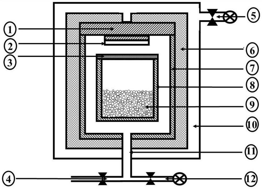
[0035] like figure 1 As shown, the present embodiment provides a device for preparing silicon carbide by PVT method, which includes a furnace body 10, an insulating layer, a growth crucible 7, a raw material crucible 8 and a porous gas permeable layer 3; the furnace body 10 is provided with an insulating layer, and the insulating layer is provided with There is a growth crucible 7, the raw material crucible 8 is located in the growth crucible 7, the porous gas permeable layer 3 is arranged at the top opening of the raw material crucible 8; the furnace body 10 is communicated with a vacuum system 5 of a furnace body 10, and the bottom of the growth crucible 7 is connected with a crucible The vacuum system 12 is in communication. The silicon carbide seed crystal 2 is grown on the bottom of the growth crucible cover 1 on the top of the growth crucible 7 .

[0036] In this embodiment, the furnace body 10 includes an upper furnace cover, a main furnace body 10 and a lower furnace ...

Embodiment 2

[0057] Using the device in the first embodiment to prepare a semi-insulating silicon carbide crystal, the steps are as follows:

[0058] 1. Add the self-made high-purity silicon carbide powder 9 into the raw material crucible 8. The particle size of the silicon carbide powder 9 ranges from 5 to 200 mesh, the purity is greater than 99.9999%, and the bulk density is 1.2 g / cm 3 . After charging, a graphite sheet with a thickness of 2 mm and a tantalum carbide coating was placed on top of the powder.

[0059] 2. Put the raw material crucible 8 in the growth crucible 7, and the growth crucible 7 is sealed with bolts and glue;

[0060] 3. Put the thermal field composed of the growth crucible 7 and the heat insulating material 6 into the furnace body 10, and the bottom of the growth crucible 7 is connected and sealed with the gas inlet and outlet pipes, and the sealing method is graphite paper with bolt pads.

[0061] 4. Close the upper and lower furnace covers and seal them throug...


PUM

PropertyMeasurementUnit
densityaaaaaaaaaa
particle sizeaaaaaaaaaa
densityaaaaaaaaaa

Abstract

The invention discloses a device and process for preparing silicon carbide through a PVT method, and relates to the technical field of silicon carbide production. The device mainly comprises a furnace body, a heat preservation layer, a growth crucible, a raw material crucible and a porous breathable layer; a heat preservation layer is arranged in the furnace body, a growth crucible is arranged in the heat preservation layer, the raw material crucible is located in the growth crucible, and the porous breathable layer is arranged at the top opening of the raw material crucible; the furnace body is communicated with a furnace body vacuum system, and the bottom of the growth crucible is communicated with a crucible vacuum system. The crucible is completely sealed, so that the crucible and an external thermal insulation material cannot be etched by a silicon-rich atmosphere, external impurities cannot enter the growth crucible, and defects such as microtubules and carbon wrapping are reduced; the cost is reduced while the service life is prolonged; the porous breathable layer is placed on the upper portion of the raw material crucible, the raw material crucible is placed on the upper portion of the growth crucible, and it is guaranteed that inlet air is evenly diffused to the upper portion of the raw material crucible from the two sides of the growth crucible while the silicon-rich atmosphere is adsorbed, so that doping stability and resistivity distribution uniformity are guaranteed.

Description

technical field [0001] The invention relates to the technical field of silicon carbide production, in particular to a device for preparing silicon carbide by PVT method and a preparation process. Background technique [0002] Silicon carbide is a third-generation semiconductor material. Compared with the first- and second-generation semiconductor materials, the third-generation semiconductor materials such as silicon carbide have a wider band gap, higher breakdown field strength, and higher thermal conductivity. Conductivity, higher electron saturation rate and higher radiation resistance, more suitable for manufacturing high temperature, high frequency, large frequency and radiation resistance devices, can be widely used in high voltage, high frequency, high temperature, high reliability and other fields, including RF communication, radar, satellite, power management, automotive electronics, industrial power electronics, etc. [0003] The preparation methods of silicon car...

Claims


Application Information

Patent Timeline
Patent Type & Authority Applications(China)
IPC IPC(8): C30B23/00C30B29/36
CPCC30B29/36C30B23/00
Inventor 刘源陈鹏飞梁刚强苗浩伟
Owner 北京清研半导科技有限公司
Learn More