Method for testing proton/single event effect resisting capacity of device

A single-event effect, proton technology, applied in electronic circuit testing, non-contact circuit testing, etc., can solve the problem of inaccurate and sensitive resistance to proton single-event effect, and achieve the effect of convenient processing

Active Publication Date: 2013-02-13
BEIJING SHENGTAOPING TEST ENG TECH RES INST
View PDF4 Cites 27 Cited by
  • Summary
  • Abstract
  • Description
  • Claims
  • Application Information

AI Technical Summary

Problems solved by technology

[0006] However, this method only analyzes and calculates the single-event turnover rate, an

Method used


Image

  • Method for testing proton/single event effect resisting capacity of device
  • Method for testing proton/single event effect resisting capacity of device
  • Method for testing proton/single event effect resisting capacity of device

Examples


Example Embodiment

[0042] The method for testing the anti-proton single event effect capability of a device proposed by the present invention is described below with reference to the accompanying drawings and examples.

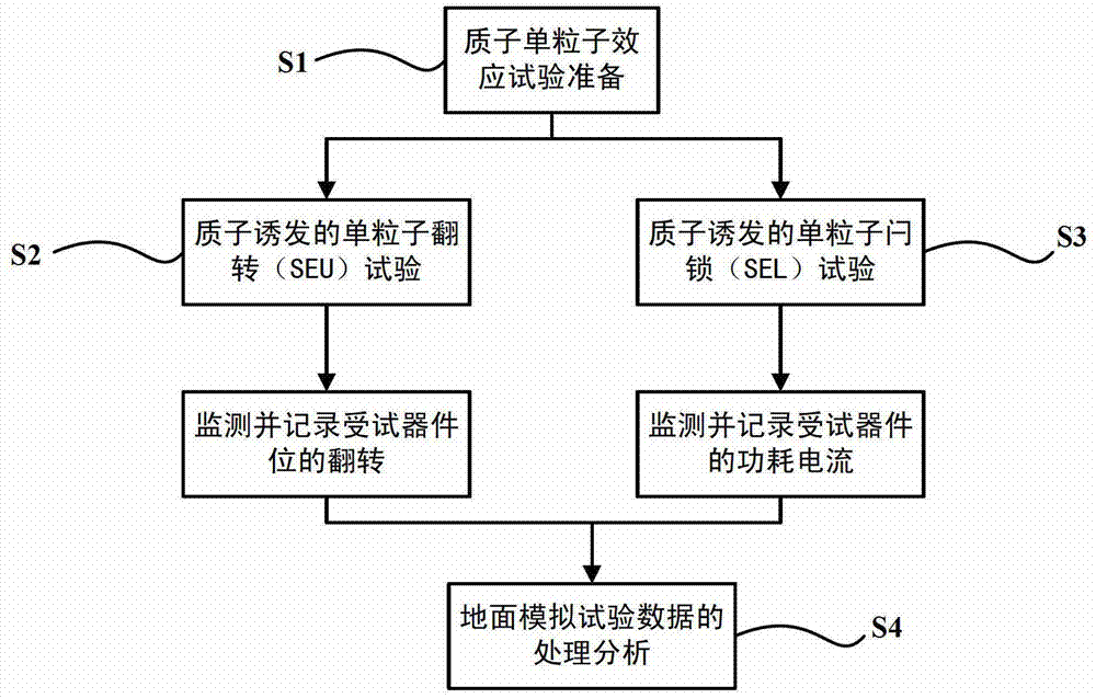
[0043] like figure 1 As shown, the proton single event effect ground simulation test method of the present invention includes the steps:

[0044] S1.1. Preparation before the proton single event effect test, prepare the device to be tested and put forward the proton single event effect test requirements;

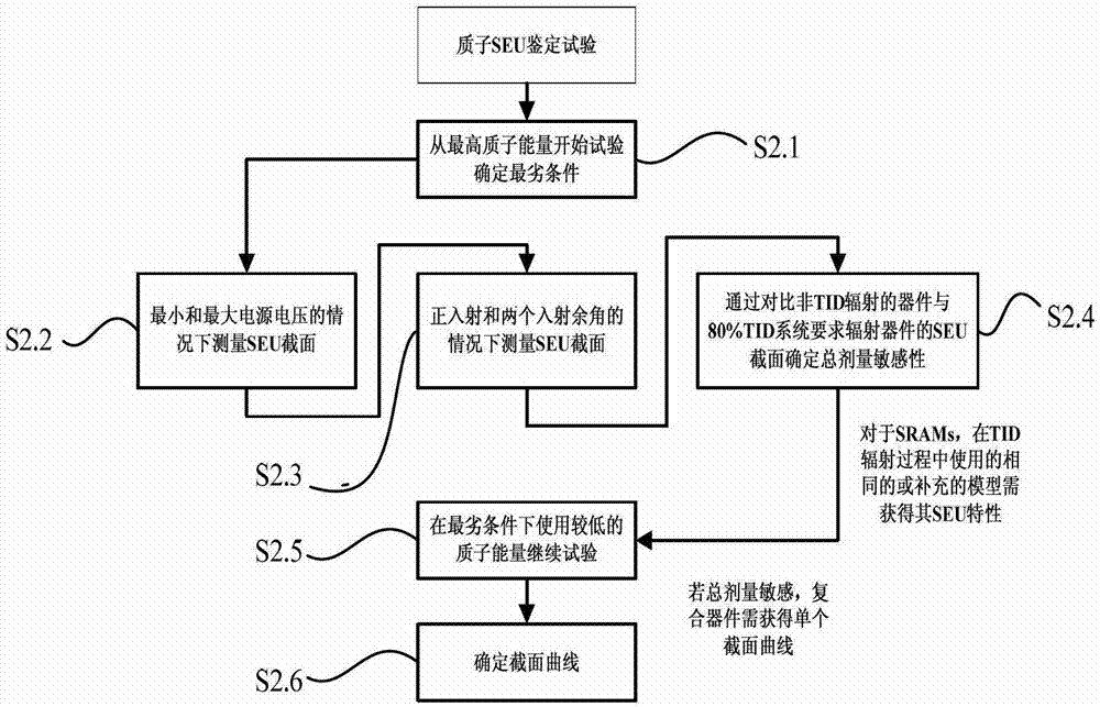
[0045] S2.1. The second step is to conduct a proton-induced single-event upset (SEU) test to monitor and record the bit flip of the device under test;

[0046] S2.2. Conduct proton-induced single-event latch-up test (SEL), monitor and record the power consumption current of the device under test;

[0047] S3.1. Process and analyze the experimental data according to the inversion data and the current and power consumption of the device to obtain the anti-proton single event e...


PUM


Abstract

The invention provides a method for testing the proton/single event effect resisting capacity of a device. The method comprises the following steps of: 1, providing the device to be tested; 2, performing proton-induced single event upset (SEU) detection to acquire the upset condition of a device position; 3, performing proton-induced signal event latchup (SEL) detection to acquire current and power consumption of the device; and 4, processing and analyzing the test data according to the upset data and the current and the power consumption of the device to acquire the proton/single event effect resisting capacity of the device. By the method, a single event effect of a space radiation environment for a semiconductor device for space navigation can be effectively and truly simulated, and the proton/single event effect resisting capacity of the device can be acquired accurately and sensitively.

Description

technical field [0001] The invention relates to the technical field of semiconductor device testing, in particular to a detection technology for the ability of aerospace semiconductor devices to resist proton single event effect. Background technique [0002] Satellite systems use a large number of semiconductor integrated circuits, such as microprocessors (CPUs), digital signal processors (DSPs), field programmable logic arrays (FPGAs), memories (Memory), and gate circuits, etc., but the semiconductors used on satellites Integrated circuits will encounter very harsh environments in space, such as radiation environment, thermal vacuum environment, micrometeor / space debris environment, etc. [0003] The space radiation environment will cause ionization damage and / or atomic displacement damage to semiconductor integrated circuits. Atomic displacement damage is the displacement of atoms after high-energy protons enter the semiconductor material, resulting in lattice defects, r...

Claims


Application Information

Patent Timeline
IPC IPC(8): G01R31/303
Inventor 王群勇冯颖阳辉陈冬梅刘燕芳白桦陈宇
Owner BEIJING SHENGTAOPING TEST ENG TECH RES INST
Why Eureka
Try Eureka