Array substrate, manufacturing method of array substrate, and display device

An array substrate and substrate technology, applied in semiconductor/solid-state device manufacturing, optics, instruments, etc., can solve problems such as alignment deviation, reduced transmittance, and light leakage, and achieve the effect of avoiding light leakage and enhancing adhesion.

Active Publication Date: 2013-02-13
BOE TECH GRP CO LTD +1
View PDF6 Cites 16 Cited by
  • Summary
  • Abstract
  • Description
  • Claims
  • Application Information

AI Technical Summary

Problems solved by technology

[0003] The inventors found that: when the array substrate and the color filter substrate are aligned to form a box, due to the limitation of the alignment accuracy, alignment deviation is very easy to occur, and the alignment devia

Method used


Image

  • Array substrate, manufacturing method of array substrate, and display device
  • Array substrate, manufacturing method of array substrate, and display device
  • Array substrate, manufacturing method of array substrate, and display device

Examples


Embodiment 1

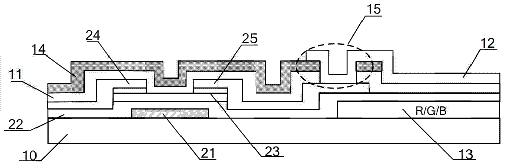
[0064] Such as figure 1 As shown, the embodiment of the present invention provides an array substrate suitable for TN products (TN mode), the array substrate includes: a substrate 10, a thin film transistor disposed on the substrate 10, a pixel electrode 12, and a passivation layer 11, the Thin film transistor comprises gate (Gate) 21, gate insulating layer (GI) 22, active layer (Active) 23, source (Source) 24 and drain electrode 25 (Drain); Passivation layer 11 covers thin film transistor, pixel electrode The device 12 is arranged above the passivation layer 11, and further includes: a patterned color resist layer 13 and a black matrix 14;

[0065] Wherein, the color resistance layer 13 is arranged between the substrate 10 and the gate insulating layer 22, and is distributed in the region corresponding to the pixel electrode 12; the black matrix 14 is arranged on the passivation layer 11, and is located in the region corresponding to the color resistance layer 13 outside the...

Embodiment 2

[0090] Embodiments of the present invention provide an array substrate suitable for ADS products (ADS mode), such as Figure 7 As shown, the difference between the array substrate and the array substrate described in Embodiment 1 is that it also includes: a common electrode 20 disposed between the substrate 10 and the color resist layer 13; in addition, because the ADS mode array substrate adopts a multi-dimensional electric field, Therefore, the pixel electrode 12 in this embodiment is in the shape of a slit, such as Figure 8 shown.

[0091] It should be noted that: the pixel electrode can be in the shape of a plate or a slit, and the same is true for the common electrode. The upper and lower order of the pixel electrode and the common electrode can be reversed, but the upper electrode must be in the shape of a slit, and the lower electrode must be in the shape of a plate. of.

[0092] Specifically, the array substrate includes: a substrate 10, a thin film transistor 16 di...

Embodiment 3

[0112] An embodiment of the present invention provides an array substrate suitable for HADS products (HADS mode), such as Figure 10 As shown, the difference from the array substrate described in Embodiment 1 is that the array substrate further includes:

[0113] The second passivation layer 26 covers the black matrix 14 and the pixel electrode 12;

[0114] The common electrode 20 is located above the second passivation layer 26 and disposed in a corresponding area of ​​the pixel electrode 12 .

[0115] In addition, because the HADS mode array substrate uses a multi-dimensional electric field, the common electrode 20 on the upper layer is in the shape of a slit, such as Figure 11 shown.

[0116] The structure of the HADS mode array substrate in this embodiment is roughly similar to the ADS mode array substrate in Embodiment 2, the only difference is that the second passivation layer 26 is added, and the common electrode 20 is arranged on the second passivation layer 26 , w...


PUM


Abstract

The invention discloses an array substrate, a manufacturing method of the array substrate, and a display device, relating to the field of displays. The influence of alignment deviation of the array substrate and a color film substrate on transmittance can be reduced to avoid the light leakage caused by the alignment deviation, and the insulativity of a signal line can be also enhanced at the same time to reduce the power consumption of a panel. The array substrate comprises a substrate, a thin film transistor arranged on the substrate, a pixel electrode and a passivation layer, wherein the passivation layer covers the thin film transistor; and the pixel electrode is arranged above the passivation layer. The array substrate further comprises a patterned color resistance layer and a black matrix, wherein the color resistance layer is arranged between the substrate and a grid insulation layer and distributed in a region corresponding to the pixel electrode; and the black matrix is arranged on the passivation layer and positioned in a region outside the region corresponding to the color resistance layer. The method comprises the steps as follows: forming a grid line and a grid; manufacturing the color resistance layer; forming the grid insulation layer, an active layer, source and drain electrode layers and the passivation layer; forming the black matrix; and forming the pixel electrode.

Description

technical field [0001] The present invention relates to the display field, in particular to an array substrate, a manufacturing method thereof, and a display device. Background technique [0002] Liquid crystal displays are now widely used in various display fields, such as households, public places, offices and personal electronic related products. At present, liquid crystal displays have developed from Twisted Nematic (TN) liquid crystal displays, which are simple to manufacture, low in cost, but have a small viewing angle, to multi-dimensional electric field (Advanced Super Dimension Switch, AD-SDS, ADS for short) liquid crystal displays. And the HADS type liquid crystal display with high aperture ratio proposed based on the ADS mode, no matter what kind of liquid crystal display, the manufacturing process of its liquid crystal panel is to manufacture the array (Array) substrate and the color filter (Color Filter) substrate separately, and then the array The substrate an...

Claims


Application Information

Patent Timeline
IPC IPC(8): G02F1/1362G02F1/1368H01L21/77
Inventor 王国磊马睿胡明
Owner BOE TECH GRP CO LTD
Why Eureka
Try Eureka