Supercharge Your Innovation With Domain-Expert AI Agents!

Photoetching technology verifying method and system thereof

A lithography process and verification method technology, applied in the field of lithography process verification, can solve the problems of low lithography process verification accuracy and large errors, and achieve the effect of improving accuracy and reducing verification errors.

Active Publication Date: 2013-02-13
CSMC TECH FAB2 CO LTD
View PDF4 Cites 0 Cited by
  • Summary
  • Abstract
  • Description
  • Claims
  • Application Information

AI Technical Summary

Problems solved by technology

[0004] In view of this, the present invention provides a lithography process verification method and system to solve the technical problems of low accuracy and large errors in lithography process verification in the prior art

Method used


Image

  • Photoetching technology verifying method and system thereof
  • Photoetching technology verifying method and system thereof

Examples


Embodiment Construction

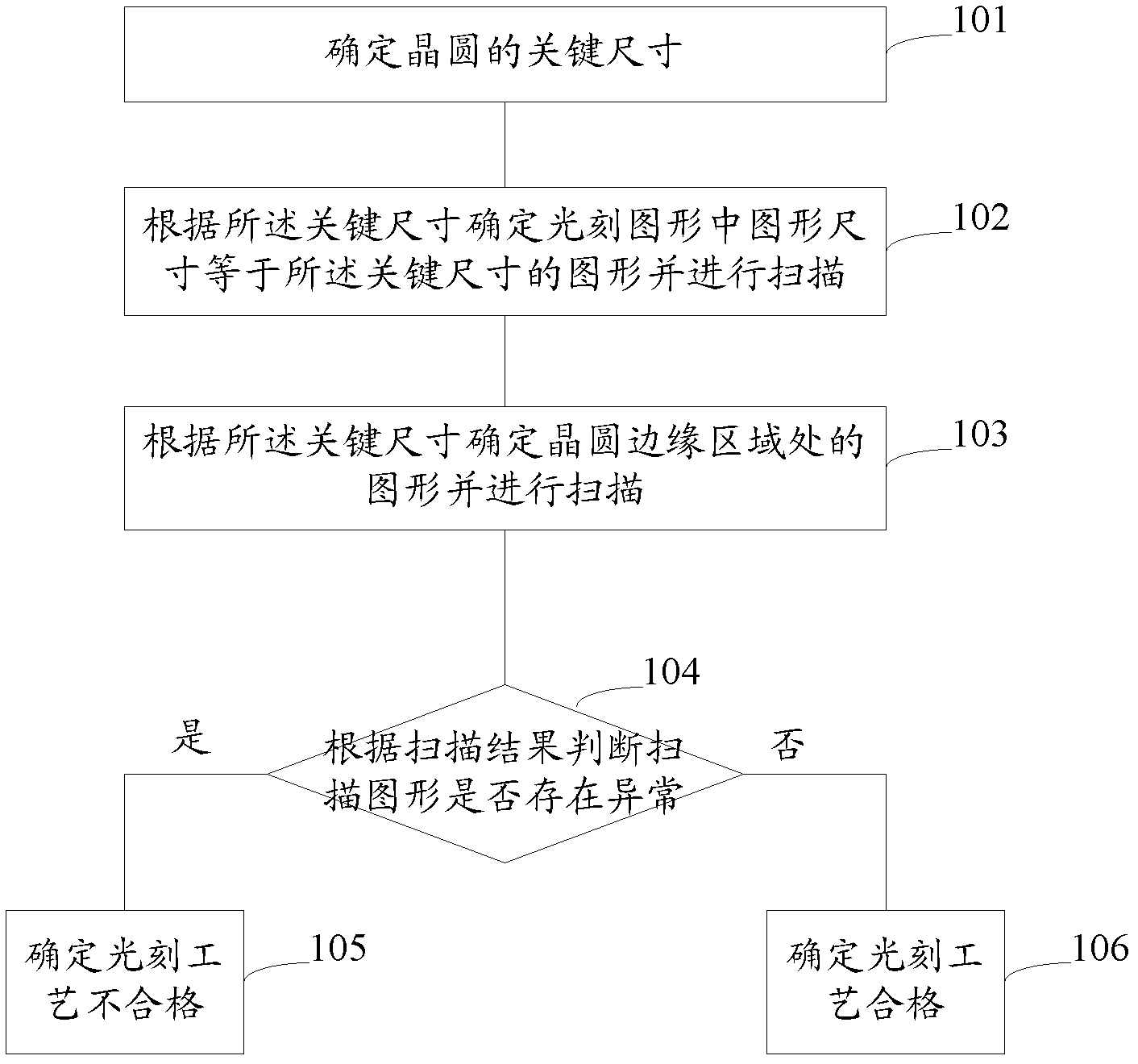
[0034] The following will clearly and completely describe the technical solutions in the embodiments of the present invention with reference to the accompanying drawings in the embodiments of the present invention. Obviously, the described embodiments are only some, not all, embodiments of the present invention. Based on the embodiments of the present invention, all other embodiments obtained by persons of ordinary skill in the art without making creative efforts belong to the protection scope of the present invention.

[0035] As mentioned in the background technology section, wafers after planarization have poor flatness. After spin-coating photoresist, exposure, and development, there are often abnormal phenomena in the pattern of poor flatness. The process verification method is only to perform routine circuit design rule detection on the pattern after lithography, and to verify the smallest size of the pattern after lithography on the wafer. Therefore, it is not accurate t...


PUM


Abstract

The invention provides a photoetching technology verifying method and a system thereof. The method comprises the following steps: determining the key dimension of a wafer; determining a photoetching figure having a figure dimension equal to the key dimension according to the key dimension, and scanning the photoetching figure; determining a figure in a wafer edge area according to the key dimension, and scanning the figure in the wafer edge area; and judging whether the scanned figures are abnormal or not according to scanning results, determining a photoetching technology is unqualified if so, and determining the photoetching technology is qualified if not. The verification of the photoetching figure in the wafer edge zone is added in the embodiment of the invention, so the photoetching technology verifying accuracy is improved.

Description

technical field [0001] The present invention relates to the technical field of semiconductors, and more specifically relates to a photolithography process verification method. Background technique [0002] With the development of semiconductor technology, the size of the wafer used for the production of silicon semiconductor integrated circuits is gradually increasing, so there is a higher requirement for the uniformity of each film layer on the wafer, and the flatness of the wafer surface is the most important factor. The uniformity of each film and the main factor of the subsequent photolithography process. [0003] The mainstream semiconductor process mainly adopts shallow trench isolation (STI) technology, and uses chemical mechanical planarization (CMP) technology to grind the wafer surface. However, due to the limitation of CMP machines, the grinding uniformity at the edge of the wafer is often poor. In the pattern formed after lithography, pattern abnormalities will ...

Claims


Application Information

Patent Timeline
Patent Type & Authority Applications(China)
IPC IPC(8): G03F7/20H01L21/00H01L21/66
Inventor 谢宝强杨兆宇赵志勇
Owner CSMC TECH FAB2 CO LTD
Features
  • R&D
  • Intellectual Property
  • Life Sciences
  • Materials
  • Tech Scout
  • Unparalleled Data Quality
  • Higher Quality Content
  • 60% Fewer Hallucinations
Learn More