Manufacturing method for semiconductor device with field barrier layer

A field blocking layer and manufacturing method technology, which is applied in semiconductor/solid-state device manufacturing, electrical components, circuits, etc., can solve the problems of low ion efficiency, high cost, and not higher than 500 degrees Celsius in the blocking layer, and achieve flexible amplification Sex and adjustability, good cost performance, cost-saving effect

Active Publication Date: 2015-02-04
SHANGHAI HUAHONG GRACE SEMICON MFG CORP
View PDF5 Cites 0 Cited by
  • Summary
  • Abstract
  • Description
  • Claims
  • Application Information

AI Technical Summary

Problems solved by technology

[0004] The existing manufacturing method of the IGBT with the field barrier layer is that after the wafer has finished the front process, according to the requirements of characteristics such as withstand voltage, the wafer is ground to the required thickness, and then the back side is implanted with ions of N-type impurities (such as phosphorus or arsenic, etc.), since there are metal materials such as AL on the front of the device at this time, the temperature used in the ordinary annealing technology generally cannot be higher than 500 degrees Celsius, and the efficiency of the implanted blocking layer ions is not activated. Therefore, it is necessary to Activated by high-temperature annealing, laser annealing can greatly improve efficiency, but the cost is high;

Method used


Image

  • Manufacturing method for semiconductor device with field barrier layer
  • Manufacturing method for semiconductor device with field barrier layer
  • Manufacturing method for semiconductor device with field barrier layer

Examples


Embodiment Construction

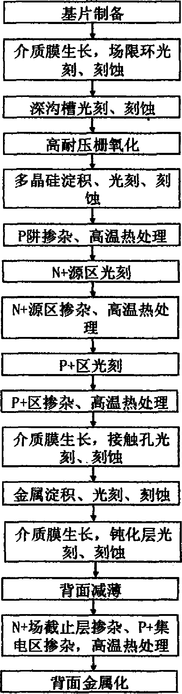
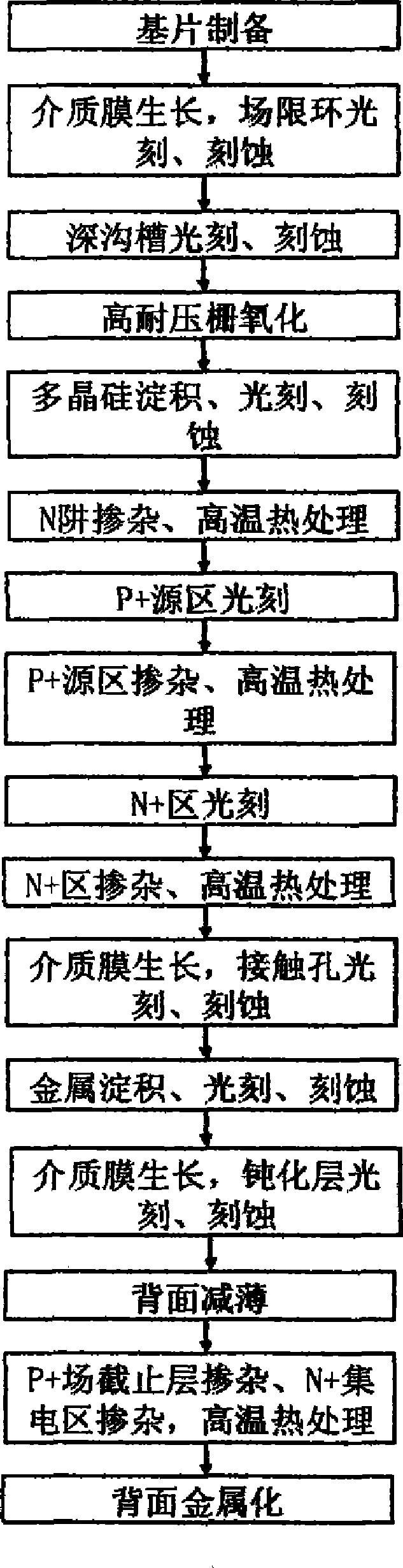
[0036] One embodiment of the method for manufacturing a semiconductor device with a field barrier layer of the present invention includes the following steps:

[0037] 1. Growing a silicon oxide film on the back of the silicon wafer, preferably, the thickness of the silicon wafer is greater than or equal to 500 microns, and the thickness of the silicon oxide film is 5000-20000 angstroms. exposure;

[0038] 2. Etching the silicon oxide film on the back of the silicon wafer to the silicon surface;

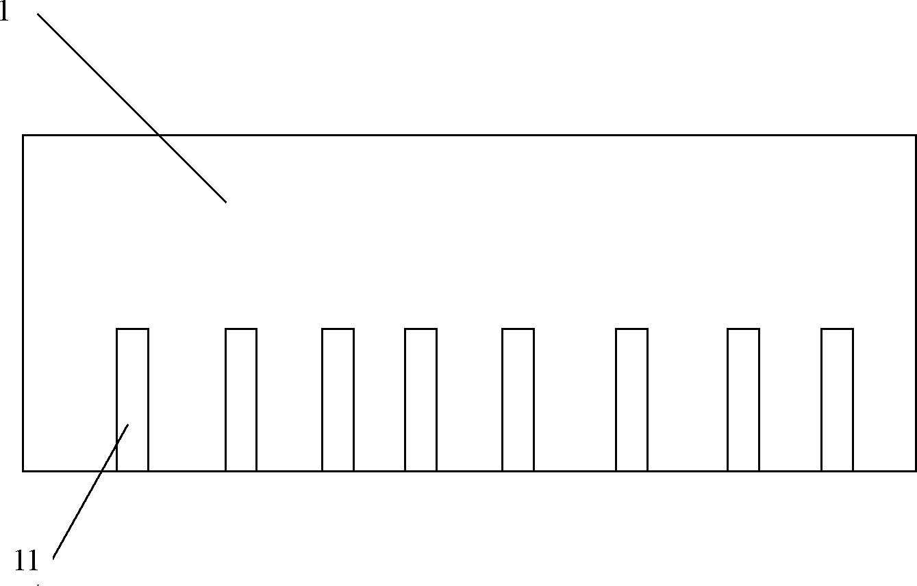
[0039] 3. Remove the photoresist, use the silicon oxide film as a barrier layer, etch silicon, etch grooves or holes of required depth on the back of the silicon wafer, and remove the silicon oxide film, preferably, the The depth of the groove or hole is greater than or equal to 20 microns;

[0040] 4. Growing highly doped polycrystalline silicon (N-type or P-type) from the groove or hole on the back of the silicon wafer, preferably, the polycrystalline concentration is greater tha...


PUM


Abstract

The invention discloses a manufacturing method for a semiconductor device with a field barrier layer. The manufacturing method comprises the following steps of etching a slot or a hole with required depth on the back of a silicon chip; growing highly doped polysilicon in the slot or the hole; diffusing at high temperature for a long time in the slot or the hole; performing the conventional positive process on the semiconductor device; and reducing the thickness of the back of the silicon chip, and leaving the required field barrier layer. According to the manufacturing method for the semiconductor device with the field barrier layer, the step of manufacturing the field barrier layer required to be subjected to high-temperature diffusion is adjusted to the front stage of a processing process of the device, a high-temperature diffusion process is not required in the silicon chip positive process, new field barrier layer structures which can confirm to different demands are easy to obtain, the problem of the limitation of the capability of a machine for processing slices is solved, the machine can finish the positive process under the condition of keeping the thickness of the silicon chip, the field barrier layer can be manufactured at deep places away from the upper surfaces of the large-size wafers, and the cost is lower.

Description

technical field [0001] The invention relates to semiconductor technology, in particular to a method for manufacturing a semiconductor device with a field barrier layer. Background technique [0002] IGBT (Insulated Gate Bipolar Transistor, Insulated Gate Bipolar Transistor), FRD (Fast Recovery Diode, Fast Recovery Diode), etc. are all semiconductor devices with a field barrier layer. [0003] IGBT (Insulated Gate Bipolar Transistor, insulated gate bipolar transistor) is a high-power power electronic device, especially for IGBTs greater than 1200 volts, it is necessary to increase the back field barrier layer to improve the withstand voltage and reduce the emission efficiency of holes. Reduce the risk of latch-up effects. At present, 4-inch or 6-inch chips are mainly used as IGBTs in the industry. Since the substrate itself is very thin, there is no major process risk. For an 8-inch wafer, the thickness of the substrate allowed by the process equipment is relatively thick, ...

Claims


Application Information

Patent Timeline
Patent Type & Authority Patents(China)
IPC IPC(8): H01L21/331H01L21/329
Inventor 张帅王海军
Owner SHANGHAI HUAHONG GRACE SEMICON MFG CORP
Why Eureka
Try Eureka