Reverse conducting IGBT (Insulated Gate Bipolar Translator) device and manufacturing method thereof

A technology of reverse conduction and devices, which is applied in the field of semiconductor devices and its manufacturing, can solve problems such as high process requirements and corrosion, and achieve the effects of high carrier mobility, fast turn-off speed, and precise impurity concentration control

Active Publication Date: 2013-02-13
JIANGSU CAS JUNSHINE TECH +1
View PDF2 Cites 3 Cited by
  • Summary
  • Abstract
  • Description
  • Claims
  • Application Information

AI Technical Summary

Problems solved by technology

However, this method requires the etching of the metal on the back, and if wet etching is used, it will corrod

Method used


Image

  • Reverse conducting IGBT (Insulated Gate Bipolar Translator) device and manufacturing method thereof
  • Reverse conducting IGBT (Insulated Gate Bipolar Translator) device and manufacturing method thereof
  • Reverse conducting IGBT (Insulated Gate Bipolar Translator) device and manufacturing method thereof

Examples


Example Embodiment

[0038] The present invention will be further described below in conjunction with specific drawings.
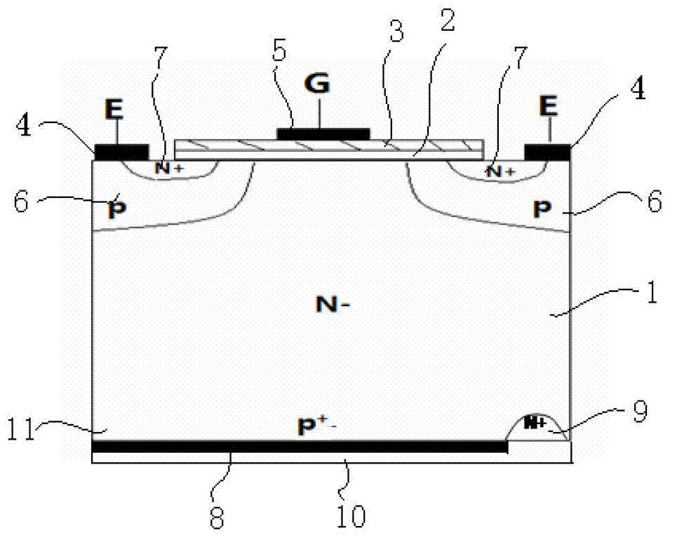
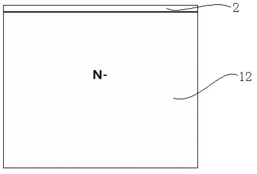
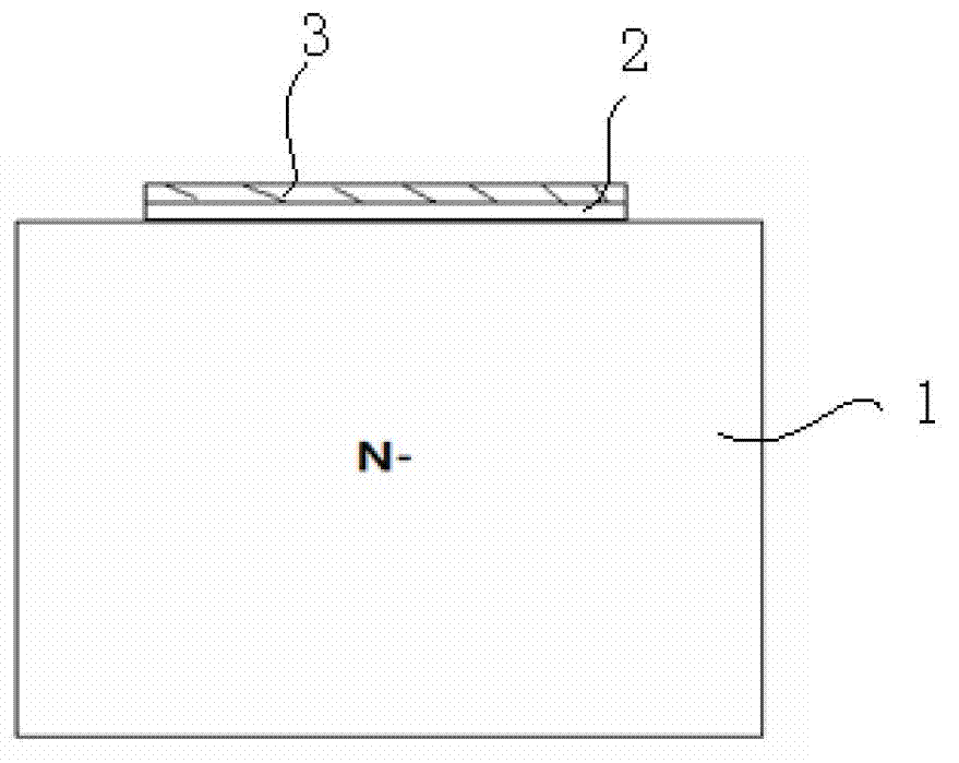
[0039] Such as Figure 1~Figure 10 Shown: Taking N-type IGBT device as an example, the present invention includes N-drift region 1, gate oxide layer 2, polycrystalline gate 3, emitter 4, gate electrode 5, P-type base region 6, N+ emitter region 7, and A collector metal region 8, an N+ collector doped region 9, a second collector metal region 10, and a P+ collector region 11.

[0040] Such as figure 1 , Picture 10 As shown, on the cross section of the IGBT device, the semiconductor substrate includes an N-drift region 1, which has a front side and a back side that are parallel to each other; a P-type base region 6 is provided in the N-drift region 1, The P-type base region 6 extends from the front to the back of the N- drift region 1, and the extension distance of the P-type base region 6 is smaller than the thickness of the N- drift region 1; the P-type base region 6 is provided ...


PUM

PropertyMeasurementUnit
Thicknessaaaaaaaaaa

Abstract

The invention relates to a reverse conducting IGBT (Insulated Gate Bipolar Translator) device which comprises a first conductive type drift region. A second conductive type base region is arranged in the first conductive type drift region. The upper part of the second conductive type base region is provided with a first conductive type emitter region; a gate oxide layer is arranged above the second conductive type base region and the first conductive type drift region; a polycrystalline gate is arranged on the gate oxide layer and provided with a gate electrode; and an emitting electrode is arranged on the second conductive type base region. The back of the first conductive type drift region is provided with a second conductive type collector region and a first conductive type collector doped region, and the first conductive type collector doped region is located at one side of the second conductive type collector region. A first collector metal region is deposited on the back of the first conductive type drift region; the second conductive type collector region is covered by one surface of the first collector metal region; a second collector metal region is deposited on the other surface of the first collector metal region; and the second conductive type collector region and the first conductive type collector doped region are covered by the second collector metal region. Through the reverse conducting IGBT device, a high impurity activation rate can be obtained at low temperature.

Description

technical field [0001] The invention relates to a semiconductor device and a manufacturing method thereof, in particular to a reverse conduction IGBT device and a manufacturing method thereof, belonging to the technical field of IGBTs. Background technique [0002] IGBT is the acronym for Insulated Gate Bipolar Transistor. It is a voltage-controlled power device and is widely used as a high-voltage switch. [0003] When the traditional IGBT is subjected to reverse voltage, the collector junction is reverse-biased and cannot be turned on. The reverse conduction IGBT allows current to flow from the emitter to the collector when the IGBT is subjected to reverse voltage. The idea of ​​reverse conduction IGBT saves chip area, packaging, and testing costs, and reduces device costs. In addition, it also has low loss, good SOA (service-oriented architecture) characteristics, positive temperature coefficient, and good soft-off characteristics, short-circuit characteristics and good...

Claims


Application Information

Patent Timeline
IPC IPC(8): H01L29/739H01L29/43H01L29/08H01L21/331H01L21/28
Inventor 徐承福朱阳军
Owner JIANGSU CAS JUNSHINE TECH
Why Eureka
Try Eureka