Split gate type flash memory and forming method thereof

A split-gate flash memory and floating gate technology, which is applied in the direction of electrical components, electric solid-state devices, circuits, etc., can solve the problems of poor working efficiency of split-gate flash memory, reduce coupling capacitance, improve coupling coefficient, and capacitive coupling capability change effect

Active Publication Date: 2013-02-20
SHANGHAI HUAHONG GRACE SEMICON MFG CORP
View PDF7 Cites 20 Cited by
  • Summary
  • Abstract
  • Description
  • Claims
  • Application Information

AI Technical Summary

Problems solved by technology

[0004] However, the existing split-gate flash memory does not work well

Method used


Image

  • Split gate type flash memory and forming method thereof
  • Split gate type flash memory and forming method thereof
  • Split gate type flash memory and forming method thereof

Examples


no. 1 example

[0025] The first embodiment of the present invention firstly provides a method for forming a split-gate flash memory, please refer to Figure 2 to Figure 11 , is a schematic structural diagram of the formation process of the split-gate flash memory according to the first embodiment of the present invention.

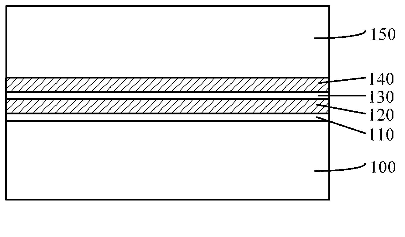
[0026] Please refer to figure 2 , a semiconductor substrate 100 is provided, a first insulating material layer 110 is formed on the surface of the semiconductor substrate 100, a floating gate material layer 120 is formed on the surface of the first insulating material layer 110, and a floating gate material layer 120 is formed on the surface of the floating gate material layer 120. The second insulating material layer 130 , a control gate material layer 140 is formed on the surface of the second insulating material layer 130 , and a mask layer 150 is formed on the surface of the control gate material layer 140 .

[0027]The semiconductor substrate 100 is selected from o...

no. 2 example

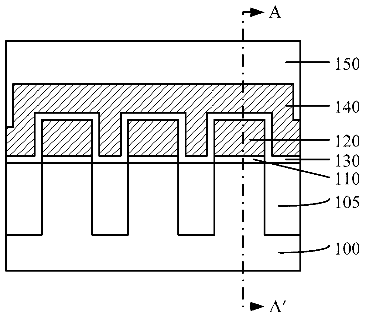
[0055] The second embodiment of the present invention also provides a method for forming a split-gate flash memory, please refer to Figure 12 to Figure 18 , is a schematic structural diagram of the formation process of the split-gate flash memory according to the second embodiment of the present invention.

[0056] In the formation process of the split-gate flash memory in the second embodiment of the present invention, the formation of the first spacer and the previous process are the same as those in the first embodiment of the present invention, please refer to Figure 2 to Figure 4 , which will not be described here.

[0057] Please refer to Figure 12 , using the first sidewall 161 as a mask, firstly etch the control gate material layer 140 and the second insulating material layer 130 to form a third opening 173 .

[0058] Please refer to Figure 13 , forming a fourth sidewall 164 on the sidewall of the third opening, using the fourth sidewall 164 as a mask to etch a ...


PUM


Abstract

The invention discloses a split gate type flash memory which comprises a semiconductor substrate, a word line, two discrete storage bit units and oxidation layers, wherein the word line is located at the bottom surface of the semiconductor substrate; the two storage bit units are located at two sides of the word line; the oxidation layers are arranged between the two storage bit units and the word line; each storage bit unit comprises a first insulation layer which is located on the bottom surface of the semiconductor substrate, a floating gate which is located on the surface of the first insulation layer, a second insulation layer which is located on the surface of the floating gate, a control gate which is located on the surface of the second insulation layer and a side wall structure which covers the floating gate and the control gate; each floating gate comprises a first floating gate and a second floating gate; and the distance between each first floating gate and the word line is greater than the distance between each second floating gate and the word line. The distance between the first floating gates and the word line is greater than the distance in the prior art, so that the coupling capacitance between the floating gates and the word line is smaller than the capacitance in the prior art, the coupling capacitance between the word line and the floating gates is as small as possible and then the erasing efficiency and the read-write efficiency of the flash memory are improved.

Description

technical field [0001] The invention relates to semiconductor technology, in particular to a split-gate flash memory and a forming method thereof. Background technique [0002] In the existing technology, flash memory (Flash) memory has become the mainstream of non-volatile semiconductor storage technology. Among various flash memory devices, there are basically two types: stacked gate flash memory and split gate flash memory. Since stacked-gate flash memory has over-erasing problems, a control gate of split-gate flash memory is also used as a select transistor (Select transistor), which effectively avoids over-erasing effects, and the circuit design is relatively simple. Moreover, compared with stacked-gate flash memory, split-gate flash memory uses source hot electron injection for programming, which has higher programming efficiency, so it is widely used in various electronic devices such as smart cards, SIM cards, microcontrollers, and mobile phones. product. [0003] ...

Claims


Application Information

Patent Timeline
Patent Type & Authority Applications(China)
IPC IPC(8): H01L27/115H01L21/8247H01L29/423
Inventor 顾靖
Owner SHANGHAI HUAHONG GRACE SEMICON MFG CORP
Why Eureka
Try Eureka