Alignment mark and its manufacturing method
A technology for alignment marks and manufacturing methods, applied in semiconductor/solid-state device manufacturing, electrical components, electric solid-state devices, etc., can solve problems such as inability to align, decrease alignment accuracy, and difficulty in obtaining alignment marks, and achieve easy access Effect
- Summary
- Abstract
- Description
- Claims
- Application Information
AI Technical Summary
Problems solved by technology
Method used
Image


Examples
Embodiment Construction
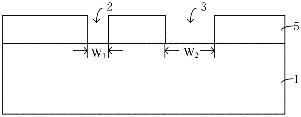
[0050] Such as Figure 4 As shown, in the prior art, the pit 91 formed on the surface of the second metal layer 9 at the position corresponding to the trench 3 is used as an alignment mark for the lithography process of the first layer metal interconnection structure. However, due to the depth of the trench 3 and the The depths of the contact holes 2 are equal and small, so the depth of the pit 91 is small, which will make it difficult to obtain the alignment marks on the silicon wafer in the subsequent lithography process, resulting in the problem of decreased alignment accuracy or inability to align .
[0051] In order to solve the above problems, the present invention forms a trench at a position corresponding to the isolation structure in the interlayer dielectric layer while forming a contact hole in the interlayer dielectric layer, and the depth of the trench extends into the isolation structure, that is, the depth of the trench The depth is greater than the depth of the...
PUM
 Abstract
Description
Claims
Application Information