Shifting register unit and array substrate gird driving device

A shift register and gate connection technology, which is applied to instruments, static indicators, etc., can solve problems such as inability to work stably for a long time

Active Publication Date: 2013-03-06
BEIJING BOE OPTOELECTRONCIS TECH CO LTD
View PDF5 Cites 68 Cited by
  • Summary
  • Abstract
  • Description
  • Claims
  • Application Information

AI Technical Summary

Problems solved by technology

In practical applications, the T2 transistor will generate noise at the output due to the influence of the coupling voltage generated by CLK, and cannot work stably for a long time

Method used


Image

  • Shifting register unit and array substrate gird driving device
  • Shifting register unit and array substrate gird driving device
  • Shifting register unit and array substrate gird driving device

Examples


Embodiment 1

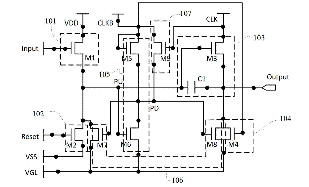
[0044] A shift register unit provided by Embodiment 1 of the present invention is suitable for bidirectional scanning, such as figure 2 As shown, the shift register unit consists of:

[0045] The input module 101, the reset module 102, the pull-up module 103, the first pull-down module 104, the second pull-down module 105 and the first pull-down control module 106 also include a second pull-down control module 107; wherein,

[0046] The input module 101 is used to provide the first working voltage VDD to the pull-up node PU point of the pull-up module in response to the input signal INPUT, wherein the pull-up node is the output node of the input module;

[0047] The reset module 102 is connected to the pull-up node, and is used for reducing the voltage of the pull-up node to the second working voltage VSS in response to the initialization signal RESET;

[0048] The pull-up module 103 is connected to the pull-up node for storing the first working voltage VDD, and in response ...

Embodiment 2

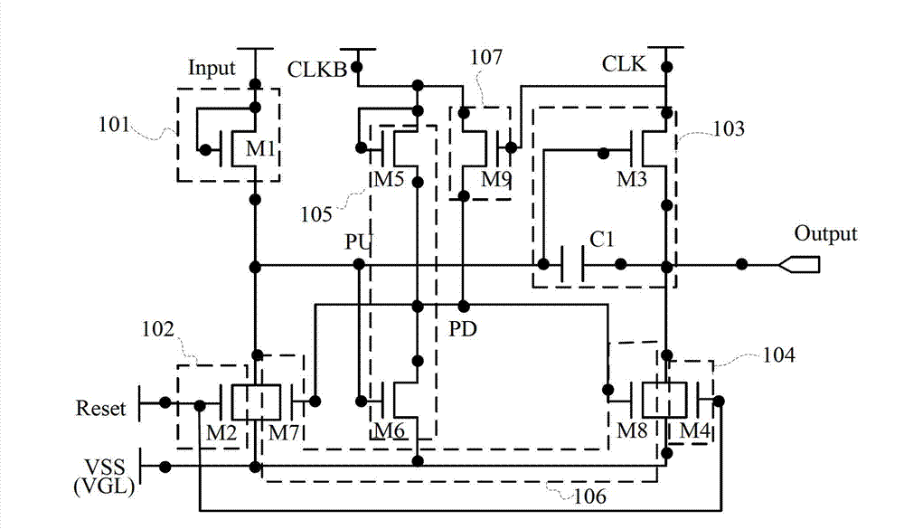
[0078] The shift register unit provided by Embodiment 2 of the present invention is also suitable for unidirectional scanning, such as image 3 As shown, when the shift register unit is used for single-phase scanning, the difference from Embodiment 1 is:

[0079] The first pull-down module 104 is configured to provide the third working voltage VGL to the output terminal OUTPUT in response to the initialization signal RESET;

[0080] Wherein the first drop-down module 104 includes:

[0081] The source of the fourth thin film transistor M4 is connected to the output terminal OUTPUT, the gate is connected to the initialization signal line RESET, and the drain is connected to the third working voltage VGL.

[0082] When the shift register unit described in Embodiment 2 of the present invention is used for single-phase scanning, refer to Figure 4 In the control signal timing diagram shown, the second working voltage VSS is the same as the third working voltage VGL, and the drivi...


PUM


Abstract

The invention discloses a shifting register unit and an array substrate gird driving device. With the adoption of the shifting register unit and the array substrate gird driving device, low-noise signals can be output by the shifting register unit and the shifting register unit can stably work for a long time period. The shifting register unit provided by the invention comprises an input module, a resetting module, a pull-upward module, a first pull-downward module, a first pull-downward control module, a second pull-downward module and a second pull-downward control module, wherein the input module is used for supplying a first working voltage to a pull-upward node of the pull-upward module; the resetting module is connected with the pull-upward node and is used for reducing the voltage of the pull-upward node to a second working voltage; the pull-upward module is connected with the pull-upward node, is used for storing the first working voltage and supplies a first clock signal to an output terminal; the first pull-downward module is used for supplying a third working voltage to the output terminal; the first pull-downward control module supplies a second clock signal to the pull-downward node, and supplies the third working voltage to the pull-downward node; the second pull-downward module is used for supplying the third working voltage to the pull-upward node and the output terminal; and the second pull-downward control module is used for inputting the second clock signal to the pull-downward node.

Description

technical field [0001] The invention relates to the technical field of liquid crystal display driving, in particular to a shift register unit and an array substrate gate driving circuit. Background technique [0002] Liquid crystal displays have the advantages of low radiation, small size, and low energy consumption, and are widely used in information products such as notebook computers, flat-screen TVs, and mobile phones. The traditional method of liquid crystal display is to use an external driver chip to drive the pixels on the panel to display images, but in order to reduce the number of components and reduce manufacturing costs, in recent years, it has gradually developed to directly fabricate the structure of the driver circuit on the display panel, for example, by The gate driving circuit is integrated in a shift register unit realized by a liquid crystal panel (gate on array, GOA) technology. [0003] However, in the GOA design of applied products, how to reduce the...

Claims


Application Information

Patent Timeline
Patent Type & Authority Applications(China)
IPC IPC(8): G09G3/36
Inventor 马磊陈东陈希
Owner BEIJING BOE OPTOELECTRONCIS TECH CO LTD
Why Eureka
Try Eureka