Pixel array substrate
A pixel array substrate and substrate technology, applied in optics, instruments, electrical components, etc., can solve problems such as high resistance value, poor display signal transmission, poor display picture quality, etc., and achieve the effect of reducing resistance
- Summary
- Abstract
- Description
- Claims
- Application Information
AI Technical Summary
Problems solved by technology
Method used
Image

Examples
Embodiment Construction
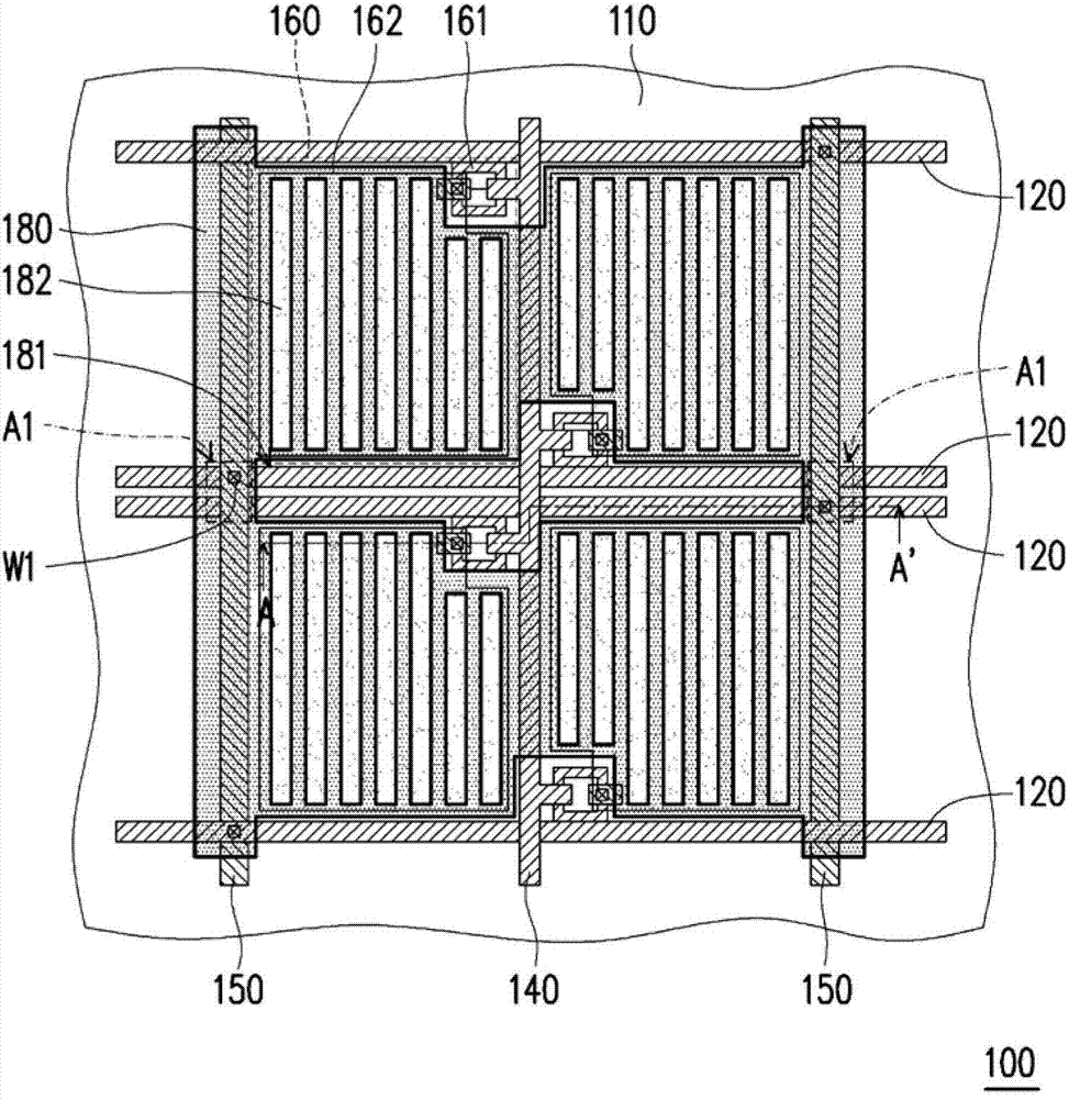
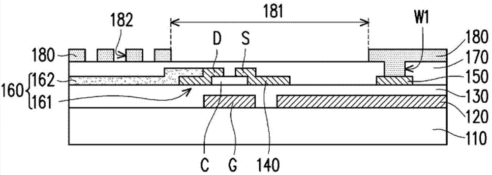
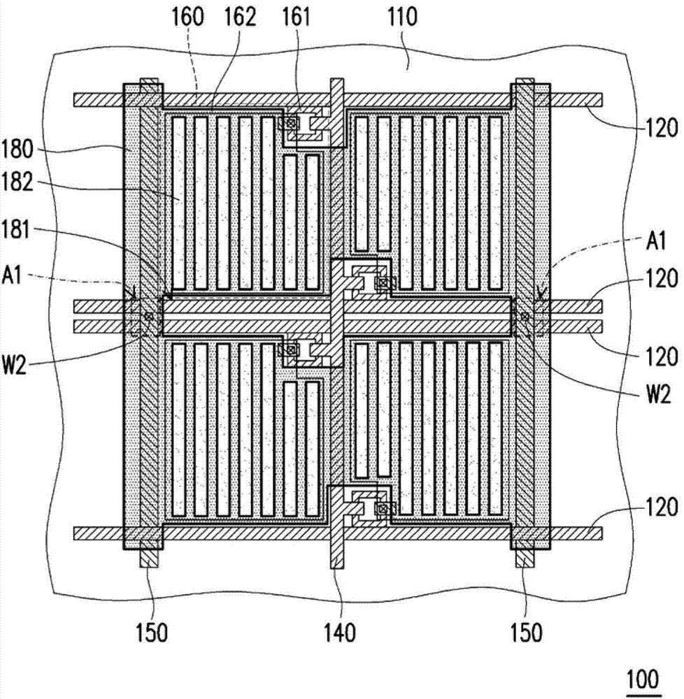
[0049] figure 1 It is a schematic partial top view of a pixel array substrate according to the first embodiment of the present invention. figure 2 yes figure 1 A partial cross-sectional schematic diagram of the pixel array substrate along the line A-A'. Please also refer to figure 1 as well as figure 2 The pixel array substrate 100 includes a substrate 110, a plurality of scanning lines 120, a first insulating layer 130, a plurality of data lines 140 (only one of which is shown in the figure), a plurality of common electrode lines 150, and a plurality of pixel structures 160 , a second insulating layer 170 and a common electrode 180 . The material of the substrate 110 can be glass, quartz or plastic, and the substrate 110 is mainly used to carry the above-mentioned other components. The aforementioned plurality of scan lines 120 are disposed on the substrate 110 , and the first insulating layer 130 covers these scan lines 120 . A plurality of data lines 140 are dispose...
PUM
 Abstract
Description
Claims
Application Information
 - R&D Engineer
- R&D Manager
- IP Professional
- Industry Leading Data Capabilities
- Powerful AI technology
- Patent DNA Extraction
Browse by: Latest US Patents, China's latest patents, Technical Efficacy Thesaurus, Application Domain, Technology Topic.
© 2024 PatSnap. All rights reserved.Legal|Privacy policy|Modern Slavery Act Transparency Statement|Sitemap