Chip for generating multiband dynamic scenes
A dynamic scene, multi-band technology, applied in color TV parts, TV system parts, TV and other directions, can solve problems such as the inability to achieve multi-band integration, and achieve simple structure, good operability, and small size. Effect
- Summary
- Abstract
- Description
- Claims
- Application Information
AI Technical Summary
Problems solved by technology
Method used
Image
Examples
Embodiment 1
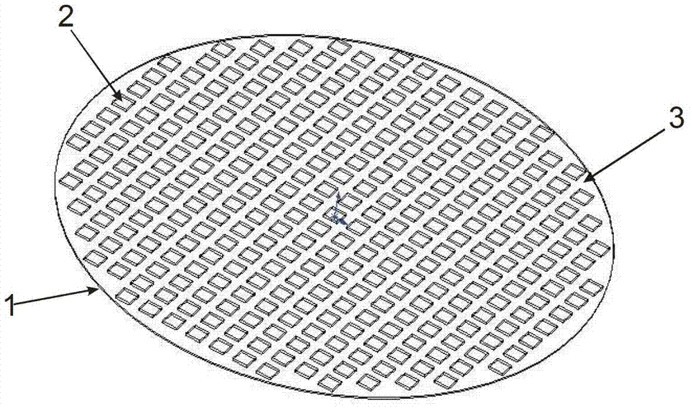
[0033] A chip for multi-band dynamic scene generation of the present invention, such as figure 1 As shown, the chip includes a substrate 1 , an infrared imaging pixel 2 and an infrared imaging pixel pitch 3 . The substrate 1 is the supporting layer of the entire chip, and a high-visible light absorbing material is fabricated on the surface of the substrate 1, and the periodically arranged high-visible light absorbing material forms an array of infrared imaging pixels 2.
[0034] The substrate 1 is made of polyimide film, and an array of infrared imaging pixels 2 is made on one side of the substrate 1 .
[0035] The thickness of the substrate 1 is 0.5 μm, the area of the substrate 1 is 50 mm in diameter, the infrared imaging pixel 2 is made of gold black, the area of the infrared imaging pixel 2 is 30 μm×30 μm, and the thickness of the infrared imaging pixel 2 is 0.5 μm. Infrared imaging pixel pitch is 20μm.
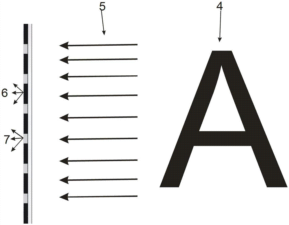
[0036] Working schematic diagram of the present invention, as ...
Embodiment 2
[0039] A chip for multi-band dynamic scene generation of the present invention, such as figure 1 As shown, the chip includes a substrate 1 , an infrared imaging pixel 2 and an infrared imaging pixel pitch 3 . The substrate 1 is the supporting layer of the entire chip, and a high-visible light absorbing material is fabricated on the surface of the substrate 1, and the periodically arranged high-visible light absorbing material forms an array of infrared imaging pixels 2.
[0040] The substrate 1 is made of polyimide film, and an array of infrared imaging pixels 2 is made on one side of the substrate 1 .
[0041] The thickness of the substrate 1 is 0.8 μm, the area of the substrate 1 is 50 mm in diameter, the infrared imaging pixel 2 adopts carbon black, the area of the infrared imaging pixel 2 is 20 μm × 20 μm, and the thickness of the infrared imaging pixel 2 is 0.3 μm, The pixel pitch of infrared imaging is 12μm.
[0042] Working schematic diagram of the present inventi...
PUM
 Abstract
Description
Claims
Application Information

