Planar array paster-type low-energy-consumption environment-friendly high-precision packaging mould for integrated circuit

A planar array, integrated circuit technology, applied in the manufacture of circuits, electrical components, semiconductor/solid-state devices, etc., can solve problems such as large warpage, gas accumulation, and unsatisfactory filling, and achieve high production efficiency, environmental protection, and production costs. reduced effect

Active Publication Date: 2013-03-20
DALIAN TAIEE PRECISION MOLD
View PDF5 Cites 4 Cited by
  • Summary
  • Abstract
  • Description
  • Claims
  • Application Information

AI Technical Summary

Problems solved by technology

[0014] In order to overcome the problems caused by the use of green epoxy plastics in existing packaging molds, the present invention provides a planar array patch type low energy consumption environment-friendly high precision integrated circuit packaging mold
This kind of mold is mainly developed for the use of green epoxy plastics. By creating a new filling process, it can avoid the backflow of green epoxy plastics and solve the problems of gas accumulation, filling dissatisfaction, and large warpage.
Solve the effect of high viscosity of green epoxy plastic on mold release by changing the release form
Eliminates failure of electrical properties such as internal delamination or cracking

Method used


Image

  • Planar array paster-type low-energy-consumption environment-friendly high-precision packaging mould for integrated circuit
  • Planar array paster-type low-energy-consumption environment-friendly high-precision packaging mould for integrated circuit
  • Planar array paster-type low-energy-consumption environment-friendly high-precision packaging mould for integrated circuit

Examples


Embodiment Construction

[0033] The structure of the present invention will be further described below with reference to the accompanying drawings.

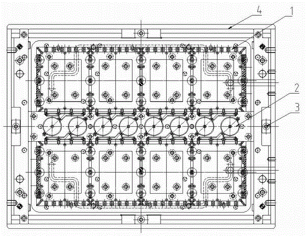
[0034] figure 1 , 2 , 3 shows a structural diagram of an upper mold box of a high-precision integrated circuit packaging mold.

[0035] Figure 4 , 5 , 6 shows a structural diagram of the lower mold box of a high-precision integrated circuit packaging mold.

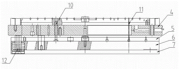
[0036] Figure 7 It shows a mold clamping structure diagram of an upper mold box and a lower mold box of a high-precision integrated circuit packaging mold.

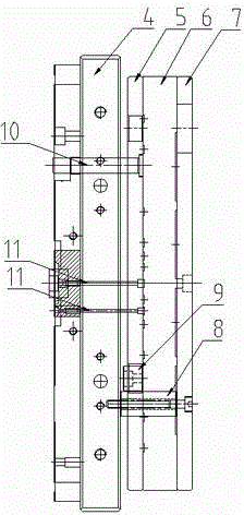
[0037] Figure 8 , 9 10 shows a structure diagram of an upper mold cavity of a high-precision integrated circuit packaging mold.

[0038] In the figure, an upper mold cavity 1, an upper mold injection block 2, and an upper mold positioning block 3 are installed on the upper mold box 4, and a lower mold cavity 13, a lower mold cavity block 14, and a lower mold cavity 19 are installed on the lower mold box 19. Injection block 15, lower ...


PUM


Abstract

The invention discloses a planar array paster-type low-energy-consumption environment-friendly high-precision packaging mould for an integrated circuit, which belongs to the technical field of semiconductor memory chip packaging. A green environment-friendly epoxy resin filling raw material can be adopted. The mould adopts a novel filling form that a plurality of lower mould material charging rods uniformly charge the material by taking a pressing machine platform oil cylinder as power, and allow green epoxy plastics to flow to an upper mould material charging block from a lower mould material charging block to be filled into an upper mould cavity, and a charging position, a size of a charging opening, and the speed and the flow rate of the charging are strictly controlled to ensure the integrity of a filling process. The problems of air accumulation, underfilling and high warping degree due to poor flowability of the green epoxy plastics in the existing mould are solved. The problem of electrical property invalidity, such as delamination or cracking, generated due to the effect of high viscosity of the green epoxy plastics on demoulding of the mould is solved by a stripping mechanism of the mould. Compared with the existing packaging form mould, the product diversification is realized; the stability is improved; and the mould has a specific significance in a wide worldwide energy conservation and consumption reduction background.

Description

technical field [0001] The invention relates to a planar array chip-type low-energy environment-friendly high-precision integrated circuit package mold, which belongs to the technical field that semiconductor memory chip packages can be filled with green and environment-friendly epoxy resin as raw materials. Background technique [0002] Epoxy resin molding compound, lead frame, chip, and gold wire are the four basic raw materials that constitute semiconductors. The main functions of the epoxy resin molding compound are: 1. Protect the chip from the influence of the external environment, and resist the influence of external moisture, solvent, and impact. 2. Good installation performance, resistance to thermal shock and mechanical vibration during installation. 3. Electrically insulate the chip from the external environment. 4. Improve heat dissipation. Therefore, epoxy resin molding compound is an indispensable main material for semiconductors. The production capacity of...

Claims


Application Information

Patent Timeline
Patent Type & Authority Applications(China)
IPC IPC(8): H01L21/56B29C45/26B29C45/14B29C45/40
Inventor 宋岩
Owner DALIAN TAIEE PRECISION MOLD
Why Eureka
Try Eureka