Large chip scale package and manufacturing method thereof

A technology for size packaging and large chips, which is applied in the field of manufacturing the large chip size packaging, can solve problems such as wafer-level processing and surface mounting technology that cannot be used at a low cost, and achieves improved warpage, increased bonding strength, and convenient The effect of the process operation

Inactive Publication Date: 2013-03-27
BEIJING UNIV OF TECH
View PDF4 Cites 17 Cited by
  • Summary
  • Abstract
  • Description
  • Claims
  • Application Information

AI Technical Summary

Problems solved by technology

Third, the package structure shown cannot be used with lowe

Method used


Image

  • Large chip scale package and manufacturing method thereof
  • Large chip scale package and manufacturing method thereof
  • Large chip scale package and manufacturing method thereof

Examples


Embodiment Construction

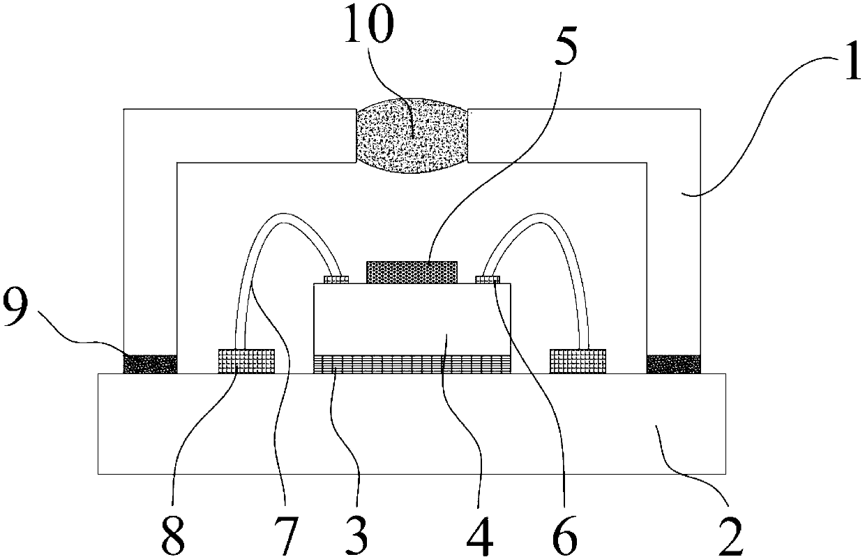
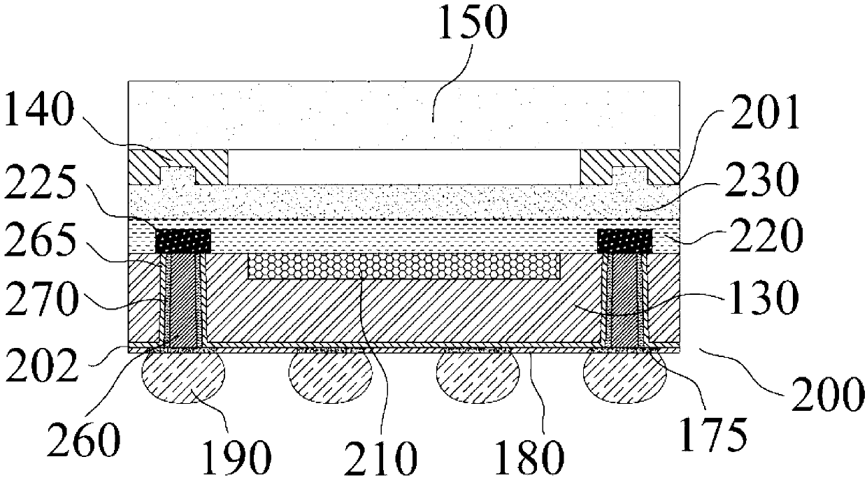
[0037] The present invention enhances the bonding force between the glass sheet 150 and the wafer 200 by making a stepped protrusion or groove structure on the first surface 201 of the wafer 200, and improves the delamination problem between the glass sheet 150 and the wafer 200 , which improves the reliability of the package and is suitable for larger size CMOS sensor (CIS) packages. FIG. 3( a ) and FIG. 3( b ) are respectively schematic diagrams of a CMOS sensor (CIS) package with stepped protrusions and grooves fabricated on the first surface 201 of the wafer.

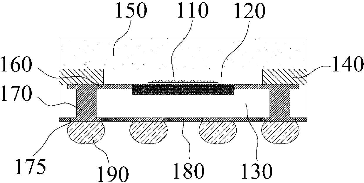
[0038] As shown in Fig. 3(a), the large chip size package according to the embodiment of the present invention includes a wafer 200, the front side of the wafer 200 is the first surface 201 forming the image sensing area, and the negative side of the wafer 200 is The second surface 202; the first surface 201 of the wafer 200 is provided with an optical interaction area 210 in the center above the silicon substrate 1...


PUM


Abstract

The invention provides large chip scale package and a manufacturing method thereof and belongs to the technical field of sensors. An optical interaction region is arranged at the center above a silicon substrate in a first surface of a wafer, one side provided with the optical interaction region is connected with a metal interconnection structure, and an input-output (I/O) around the optical interaction region on the silicon substrate is connected to an electrode pad through the metal interconnection structure. The surface of the metal interconnection structure is provided with a protective layer, and a stepped protrusion or groove structure is formed on the protective layer. The first surface of the wafer is bonded with a glass piece together, and a cavity is formed between the glass piece and the wafer. A second surface of the wafer is provided with a through silicon via (TSV) hole, the electrode pad penetrates through the silicon substrate through the TSV hole to be connected to a bonding pad on the second surface of the wafer, a passivation layer and a metal liner are sequentially manufactured on a hole wall of the TSV hole, and a polymer material is filled into the TSV hole. An anti-welding layer is manufactured on the second surface of the wafer, and a weld ball is manufactured on the bonding pad. By means of the large chip scale package and the manufacturing method, the layering problem of glass and the silicon substrate in an existing package structure is solved, and the packing reliability is improved.

Description

technical field [0001] The present invention relates to a large chip size package (CSP) and a method of manufacturing the same. The packaging structure and manufacturing method described above can be preferably used for image sensors or MEMS devices. Background technique [0002] Chip Scale Package (CSP) is a new generation of chip packaging technology, and its technical performance has been improved again. CSP packaging can make the ratio of chip area to package area exceed 1:1.14, which is quite close to the ideal situation of 1:1. The absolute size is only 32 square millimeters, about 1 / 3 of ordinary BGA, which is only equivalent to TSOP memory 1 / 6 of the chip area. Compared with the BGA package, the CSP package can increase the storage capacity by three times in the same space. The purpose of CSP is to use large chips (chips with more functions, better performance, and more complex chips) to replace the previous small chips, while the package occupies the same or smal...

Claims


Application Information

Patent Timeline
IPC IPC(8): H01L27/146
Inventor 秦飞武伟安彤刘程艳陈思夏国峰朱文辉
Owner BEIJING UNIV OF TECH
Why Eureka
Try Eureka