LED chip and manufacture method thereof
A LED chip and epitaxy technology, which is applied in semiconductor devices, electrical components, circuits, etc., can solve the problems of epitaxial luminous body splits and differences in thermal expansion coefficients, and achieve the effects of improving thermal mismatch problems, increasing yields, and improving split problems
- Summary
- Abstract
- Description
- Claims
- Application Information
AI Technical Summary
Problems solved by technology
Method used
Image
Examples
Embodiment Construction
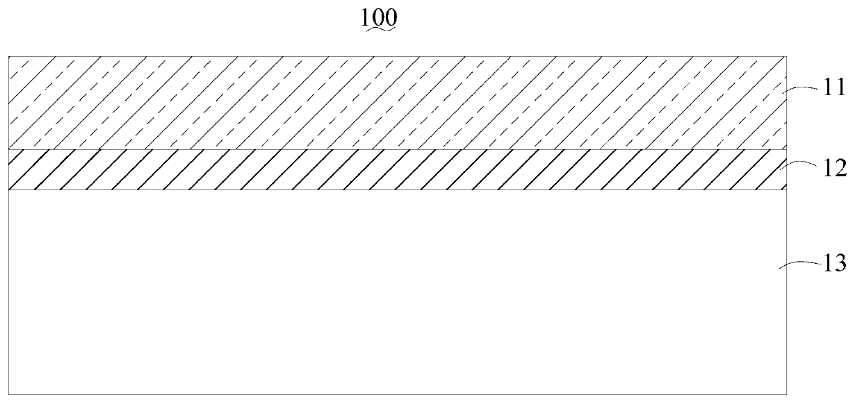
[0025] refer to figure 1 , the LED chip 100 according to the first embodiment of the present invention includes an epitaxial luminous body 11 , a thermally conductive buffer layer (not shown) and a thermally conductive substrate 13 .
[0026] The epitaxial luminous body 11 is grown from a sapphire or silicon carbide substrate (not shown) and forms an existing LED chip (not shown) therewith. In order to improve the heat dissipation performance of the existing LED chip, the epitaxial luminous body 11 is peeled off from the sapphire or silicon carbide substrate for later use.
[0027] The thermally conductive substrate 13 is a metal or ceramic substrate whose heat dissipation performance is better than that of sapphire and silicon carbide. In this embodiment, the thermally conductive substrate 13 is flat. The thermally conductive buffer layer is disposed on one side of the thermally conductive substrate 13 . In this embodiment, the thermally conductive buffer layer is the therm...
PUM
 Abstract
Description
Claims
Application Information


