A method for improving back side stress of an IGBT

A technology of stress and silicon wafer surface, which is applied in the manufacture of electrical components, electrical solid devices, semiconductor/solid devices, etc., can solve the problems of easy cracking of silicon wafers, and achieve the effect of reducing stress and improving split problems

Inactive Publication Date: 2016-12-14
SHANGHAI HUAHONG GRACE SEMICON MFG CORP
View PDF3 Cites 6 Cited by
  • Summary
  • Abstract
  • Description
  • Claims
  • Application Information

AI Technical Summary

Problems solved by technology

[0005] The technical problem to be solved by the present invention is to provide a method for improving the stress of the IGBT, and to solve the problem that silicon wafers are easily cracked in the scribing area

Method used


Image

  • A method for improving back side stress of an IGBT
  • A method for improving back side stress of an IGBT
  • A method for improving back side stress of an IGBT

Examples


Embodiment Construction

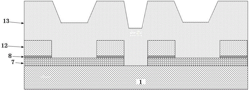
[0027] The method for improving IGBT stress described in the present invention, such as image 3 and Figure 4 As shown, for the polyimide 12 covered on the passivation layer on the front side of the silicon wafer, after photolithography and etching patterning, a layer of blue film 13 with a thickness of 100-350 μm is pasted on the entire surface of the silicon wafer. The blue film 13 is fully filled in the depressions and gaps after polyimide etching and patterning, and the softer blue film is attached to the surface of the silicon wafer, and its surface is also convex with the shape of the polyimide. Rigid or sunken, the surface has undulations and is not smooth enough. Then the blue film 13 is ground to make the surface flat, as Figure 4 As shown, a stress buffer layer is formed.

[0028] The method for improving the back stress of the IGBT according to the present invention comprises the steps of:

[0029] The first step is to attach the blue film to the front of the ...


PUM


Abstract

The invention discloses a method for improving back side stress of an IGBT. After lithography and etching patterning are carried out on polyimides covering a passivation layer on the front surface of a silicon chip, a blue membrane covers the surface of the whole silicon chip. Afterwards, grinding is carried out on the blue membrane to enable the blue membrane to be flattened. According to the invention, the relatively soft blue membrane is fully filled in the slits or pattern depressed areas of the silicon chip to form a stress buffer layer; stress in high-step areas in a grinding process is reduced; and problems of cracking due to back side stress is effectively alleviated.

Description

technical field [0001] The invention relates to the field of design and manufacture of integrated circuits, in particular to a method for improving the back stress of an IGBT. Background technique [0002] IGBT (Insulated Gate Bipolar Transistor) Insulated Gate Bipolar Transistor is a composite fully-controlled voltage-driven power semiconductor device composed of BJT (Bipolar Transistor) and MOS (Insulated Gate Field Effect Transistor). The advantages of high input impedance and low conduction voltage drop of GTR. It is very suitable for the conversion system with a DC voltage of 600V and above, such as AC motors, frequency converters, switching power supplies, lighting circuits, traction drives and other fields. [0003] Common IGBT structures such as figure 1 As shown, the front side of substrate 1, namely figure 1 The upper part is the gate 2 on the front of the IGBT, the gate oxide layer 3, the P well 4, the front metal connection 7 and so on. the back, ie figure 1...

Claims


Application Information

Patent Timeline
Patent Type & Authority Applications(China)
IPC IPC(8): H01L21/683
CPCH01L21/6835H01L2221/68331
Inventor 马彪黄璇
Owner SHANGHAI HUAHONG GRACE SEMICON MFG CORP
Why Eureka
Try Eureka