Controllable heating and defrosting capacitive type high-altitude humidity sensor and manufacturing method thereof
A humidity sensor and temperature sensor technology, which is applied in the fields of material capacitance, manufacturing microstructure devices, decorative art, etc., can solve the problems of sensor frosting, affecting humidity data collection, etc., and achieve the effect of improving accuracy
- Summary
- Abstract
- Description
- Claims
- Application Information
AI Technical Summary
Problems solved by technology
Method used
Image
Examples
specific Embodiment approach 1
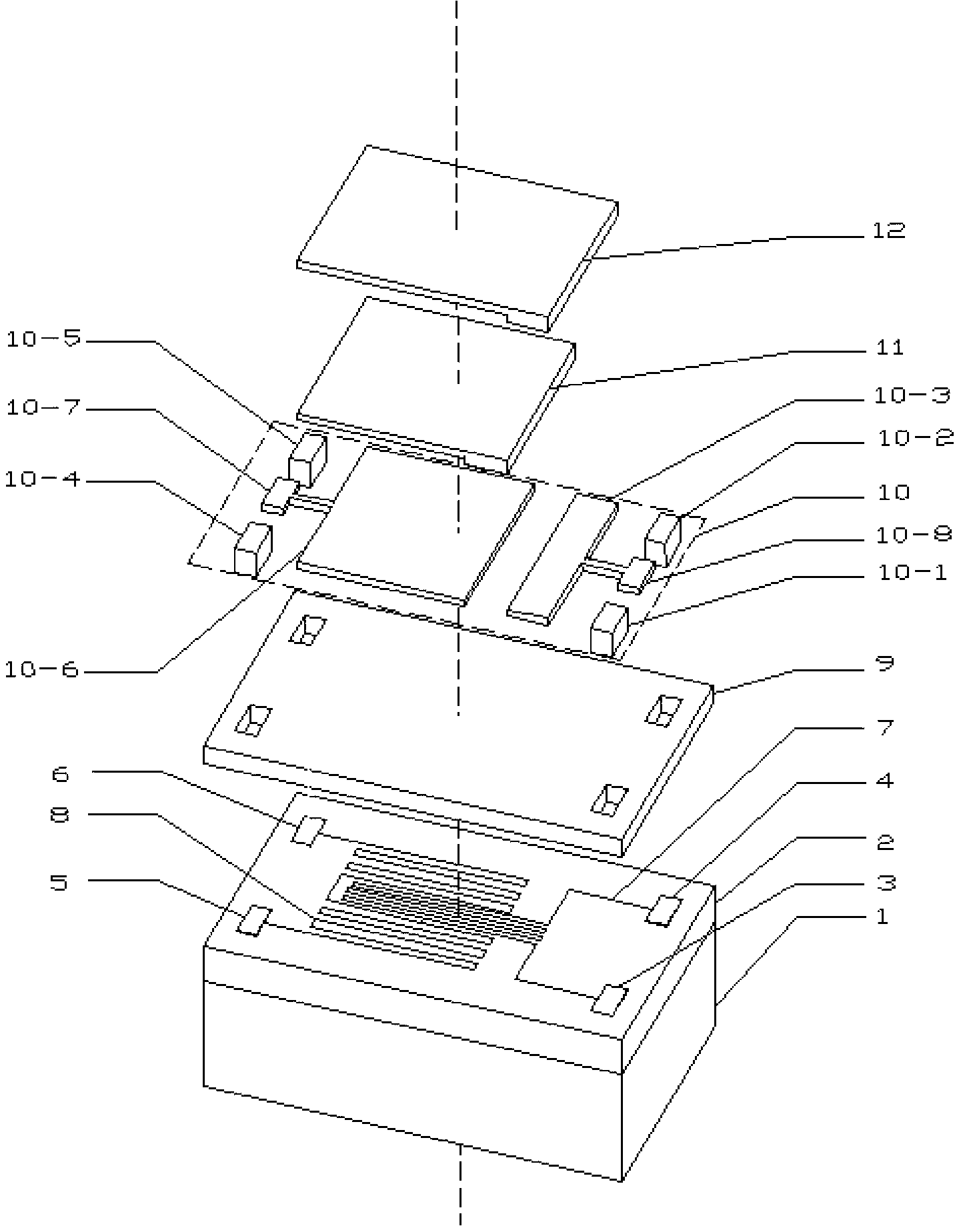
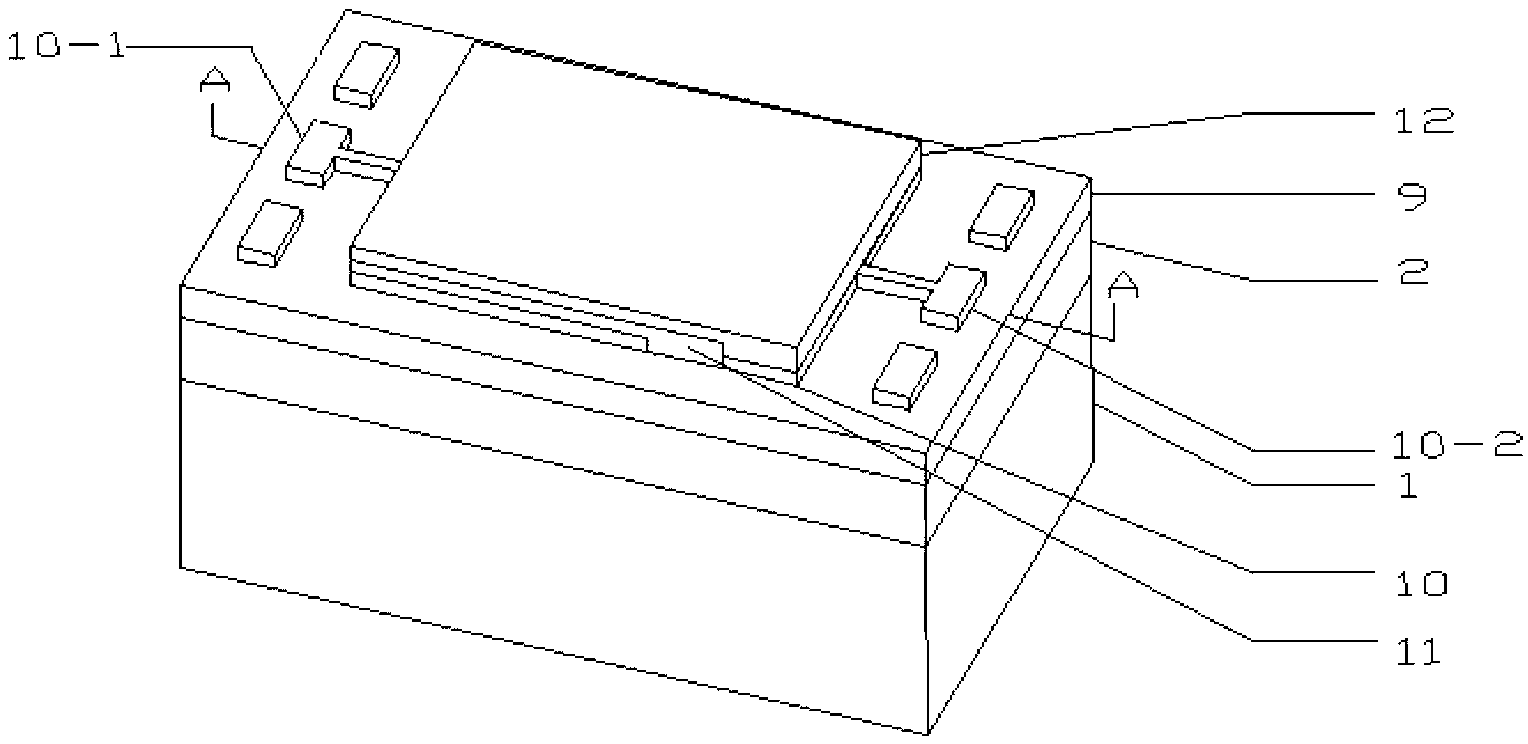
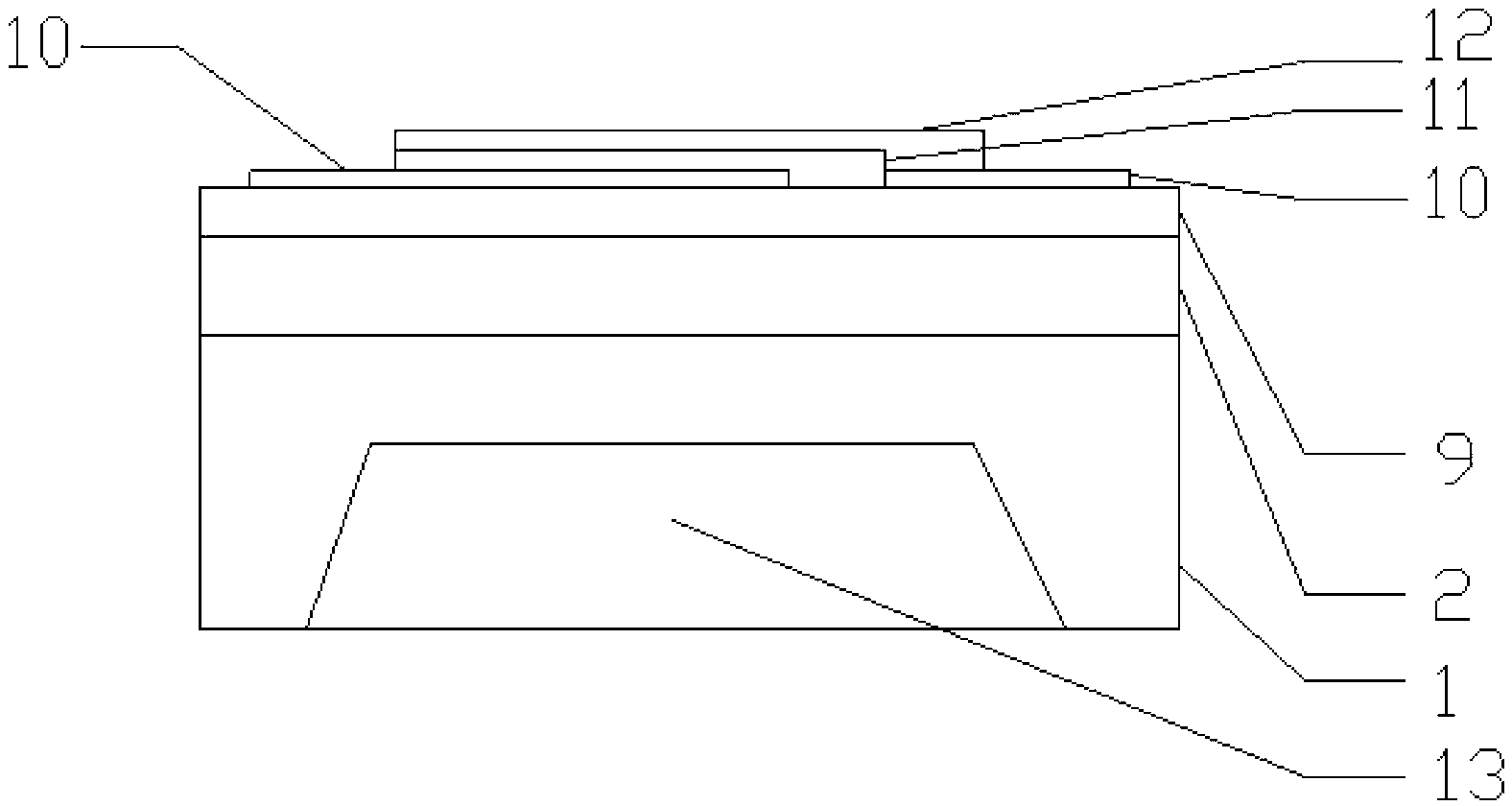
[0022] Specific implementation mode one: combine figure 1 , figure 2 , image 3 and Figure 4 , this embodiment is a controllable heating and defrosting capacitive high-altitude humidity sensor, including a substrate 1, a first insulating layer 2, a first temperature sensor pad 3, a second temperature sensor pad 4, and a first heater pad 5. The second heater pad 6, the temperature sensor electrode 7, the heater electrode 8, the second insulating layer 9, the lower electrode 10, the moisture sensing layer 11, the porous upper electrode 12 and the groove 13; The first insulating layer 2 is laid on the surface; a temperature sensor electrode 7 and a heater electrode 8 are arranged on the upper surface of the first insulating layer 2, and the first temperature sensor pad 3 and the second electrode are connected to the two ends of the temperature sensor electrode 7. The temperature sensor pad 4 is connected to the first heater pad 5 and the second heater pad 6 at both ends of t...
specific Embodiment approach 2
[0031] Specific implementation mode 2: This implementation mode is a preparation method of a controllable heating and defrosting capacitive high-altitude humidity sensor, which is specifically completed according to the following steps:
[0032] 1. Prepare a silicon wafer with a crystal orientation of [100] and a thickness of 150 μm to 250 μm as the substrate 1, and clean the surface of the substrate 1;
[0033] 2. The surface of the silicon wafer is oxidized, and a layer of dense SiO is obtained on the surface of the silicon wafer 2 layer, namely the first insulating layer 2;
[0034] 3. Prepare temperature sensor electrodes 7 and heater electrodes 8 on the upper surface of the substrate processed in step 2 by photolithography stripping method, connect the two ends of the temperature sensor electrodes 7 to the first temperature sensor pad 3 and the second temperature sensor respectively The two ends of the heater electrode 8 are connected to the first heater pad 5 and the se...
specific Embodiment approach 3
[0041] Embodiment 3: The difference between this embodiment and Embodiment 2 is that the thickness of the first insulating layer 2 is 500 nm to 1000 nm. Others are the same as in the second embodiment.
PUM
| Property | Measurement | Unit |
|---|---|---|
| Thickness | aaaaa | aaaaa |
| Resistance | aaaaa | aaaaa |
| Resistance | aaaaa | aaaaa |
Abstract
Description
Claims
Application Information


