High-temperature wafer level burn-in test scheduling method for SoC (system on a chip) chip

A test scheduling and aging test technology, applied in the field of integrated circuits, can solve problems such as insufficient reliability tests, save test costs, improve accuracy, and reduce the requirements of test equipment.

Inactive Publication Date: 2013-04-03
PEKING UNIV SHENZHEN GRADUATE SCHOOL +1
View PDF0 Cites 14 Cited by
  • Summary
  • Abstract
  • Description
  • Claims
  • Application Information

AI Technical Summary

Problems solved by technology

When the ambient temperature is applied to the SoC chip, some IP reliability tests may be insufficient, and some IP may be subjected to excessive stress

Method used


Image

  • High-temperature wafer level burn-in test scheduling method for SoC (system on a chip) chip
  • High-temperature wafer level burn-in test scheduling method for SoC (system on a chip) chip
  • High-temperature wafer level burn-in test scheduling method for SoC (system on a chip) chip

Examples


Embodiment Construction

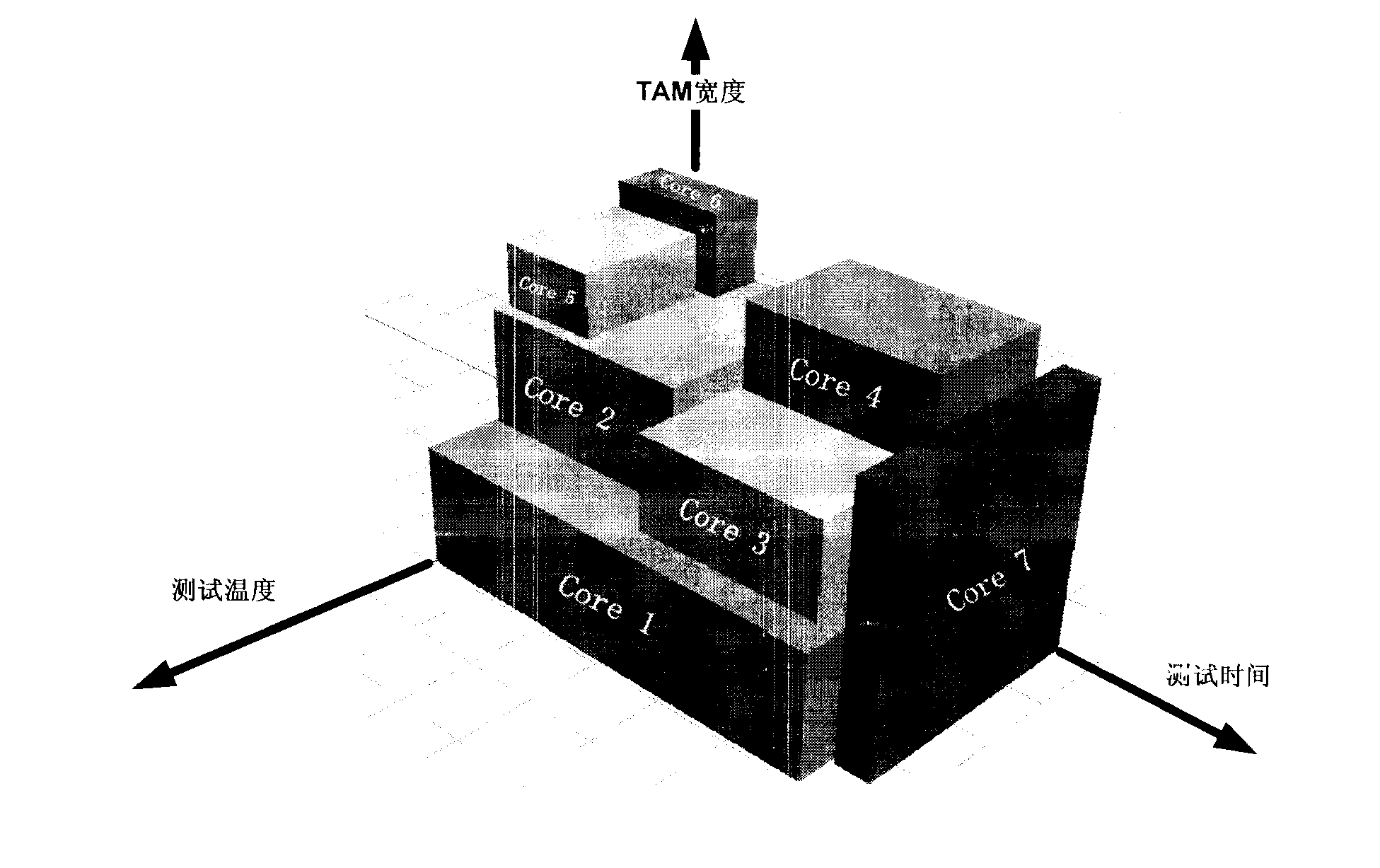
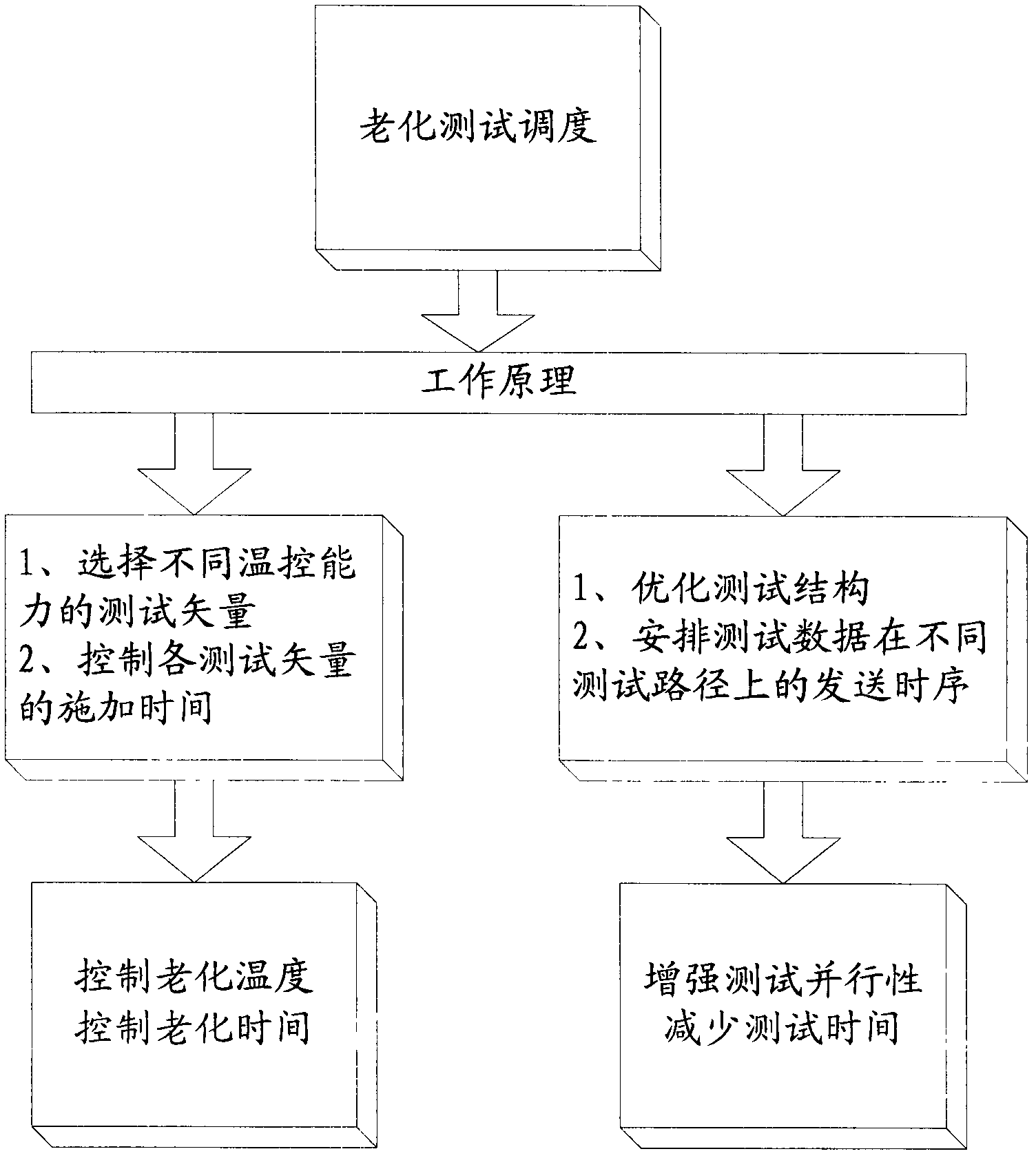
[0017] The needs of the present invention are implemented according to the following 4 steps:

[0018] first step:

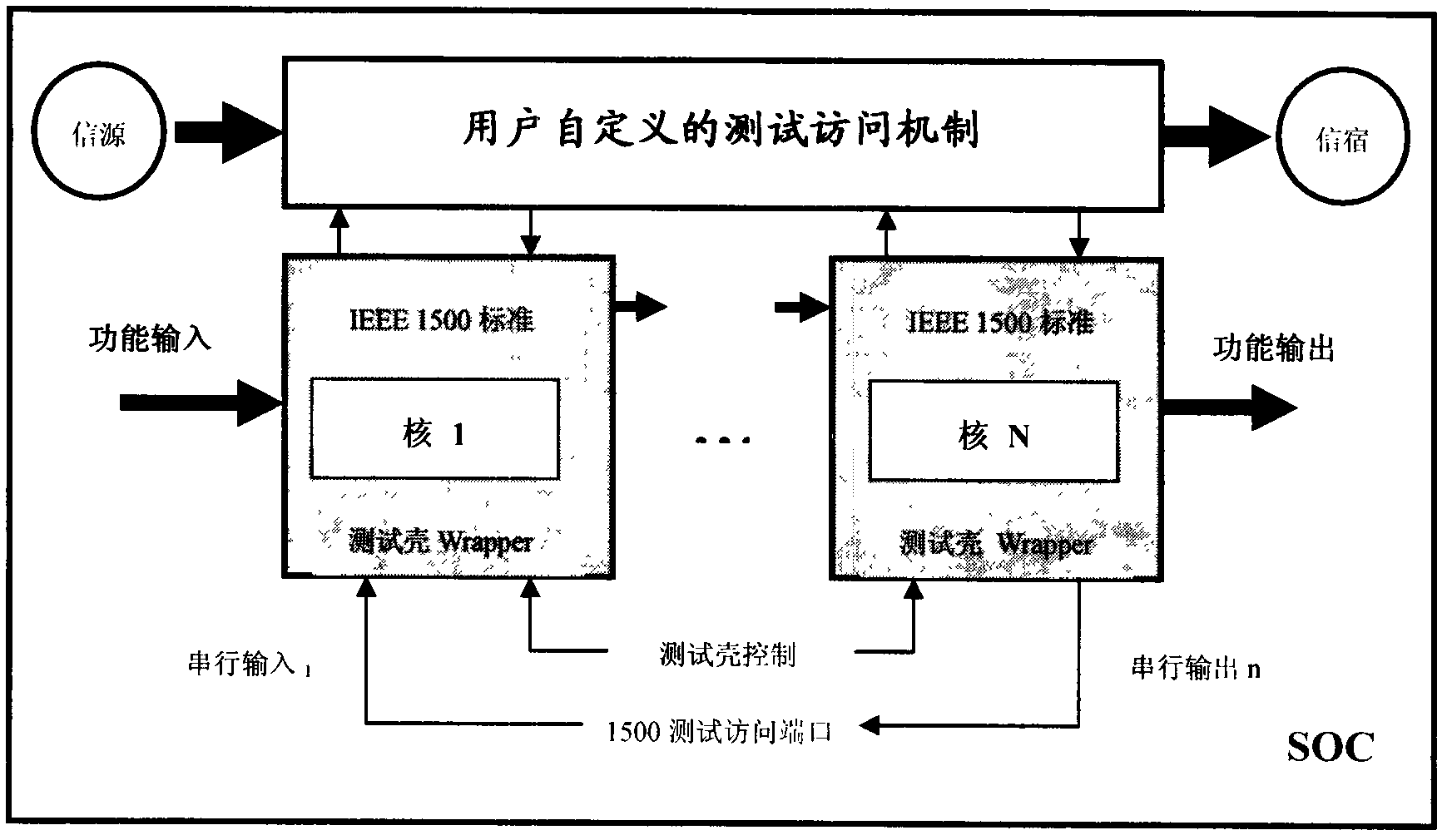
[0019] Obtain information such as process documents, wafer material parameters, wafer layout and dimensions, burn-in test requirements, etc.

[0020] Step two:

[0021] Calculate the effect of different test input vectors on the power consumption and temperature control of the chip, and obtain the test vector sets corresponding to different temperature rise conditions.

[0022] Circuit power consumption P is mainly composed of dynamic power consumption and static power consumption.

[0023] The dynamic power consumption of the circuit is determined by formula (1):

[0024] P dyn =1 / 2·C·V 2 · N · f(1)

[0025] Among them, V is the operating voltage of the circuit, C is the load capacitance of the circuit, f is the operating frequency, and N is the number of circuit level jumps. After the circuit is made, the circuit load capacitance C is basically unchange...


PUM


Abstract

The invention discloses a high-temperature wafer level burn-in test scheduling method for an SoC (system on a chip) chip. The high-temperature wafer level burn-in test scheduling method comprises the steps of heating a chip by utilizing high heat produced by the chip in the test mode, and controlling the application time of every test vector by taking the power dissipation of a circuit node as orientation and selecting test vectors with different temperature control functions so as to control the test temperature of a circuit module or the SoC chip and control the WLTBI (wafer level test and burn-in) test lasting time; and arranging the sending time sequence of test data in different test paths so as to enhance the test parallelism and reduce the test time. The high-temperature wafer level burn-in test scheduling method for the SoC chip can flexibly configure test schemes under the same test according to the test requirements, so that the aims of enhancing the accuracy of the burn-in test and the cost of the test can be achieved.

Description

technical field [0001] The invention relates to the technical field of integrated circuits, in particular to a wafer-level aging test method for integrated circuits. Background technique [0002] In order to make chip products go through the early failure stage of the "bathtub curve" of its failure rate before delivery to users, it is necessary to perform aging tests on chips. WLTBI (Wafer Level Test during Burn In) technology simultaneously performs chip fault coverage test (usually for fixed faults, Stuck-At Faults) and burn-in test on the wafer surface, which has a significant effect on improving chip production yield and reducing chip cost , the International Technology Roadmap for Semiconductors (ITRS: International Technology Roadmap for Semiconductors) has listed it as one of the important development parties in today's chip testing technology. The chip packaging test after adopting WLTBI technology is significantly different from the traditional chip packaging test ...

Claims


Application Information

Patent Timeline
Patent Type & Authority Applications(China)
IPC IPC(8): G01R31/26
Inventor 崔小乐李崇仁程伟陶玉娟
Owner PEKING UNIV SHENZHEN GRADUATE SCHOOL
Why Eureka
Try Eureka