Array substrate and manufacture method thereof

A technology of array substrates and substrate substrates, which is applied in semiconductor/solid-state device manufacturing, optics, instruments, etc., can solve problems such as low efficiency and complicated manufacturing processes, and achieve the effects of reducing manufacturing costs, simplifying manufacturing processes, and improving manufacturing efficiency

Active Publication Date: 2013-04-03
BOE TECH GRP CO LTD
View PDF4 Cites 18 Cited by
  • Summary
  • Abstract
  • Description
  • Claims
  • Application Information

AI Technical Summary

Problems solved by technology

[0007] The embodiment of the present invention provides an array substrate and a manufacturing method thereof, which are used to solve the problems in the prior art that TFT-LCDs based on the ADS structure usually need to go through 4 or 5 masking processes, the manufacturing process is complicated, and the efficiency is low.

Method used


Image

  • Array substrate and manufacture method thereof
  • Array substrate and manufacture method thereof
  • Array substrate and manufacture method thereof

Examples


Embodiment Construction

[0043] Embodiments of the present invention provide an array substrate and a manufacturing method thereof, which not only improve the characteristics of the TFT-LCD array substrate, but also reduce manufacturing costs.

[0044] The embodiments of the present invention will be further described in detail below in conjunction with the accompanying drawings.

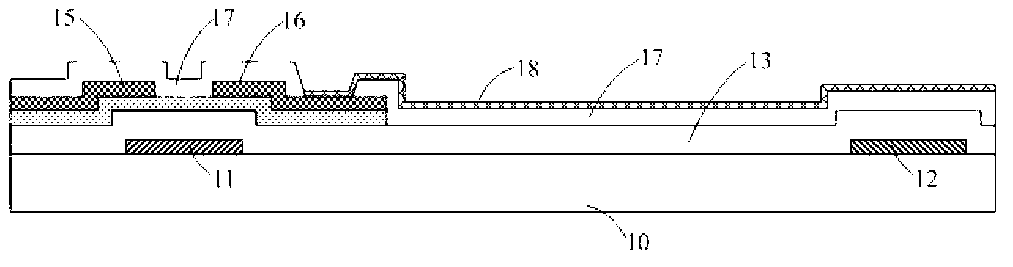
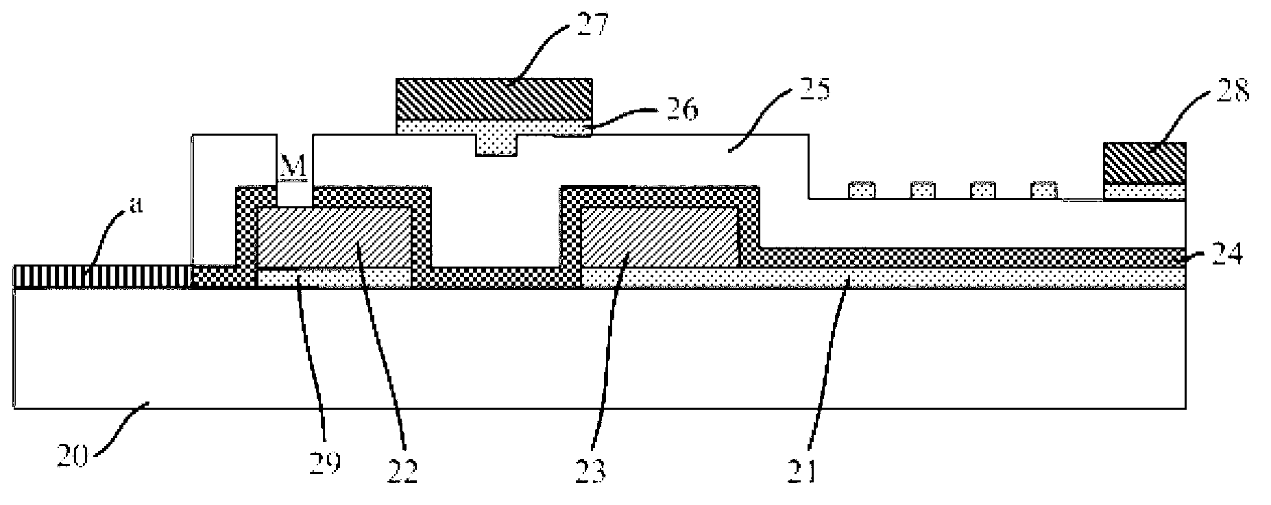
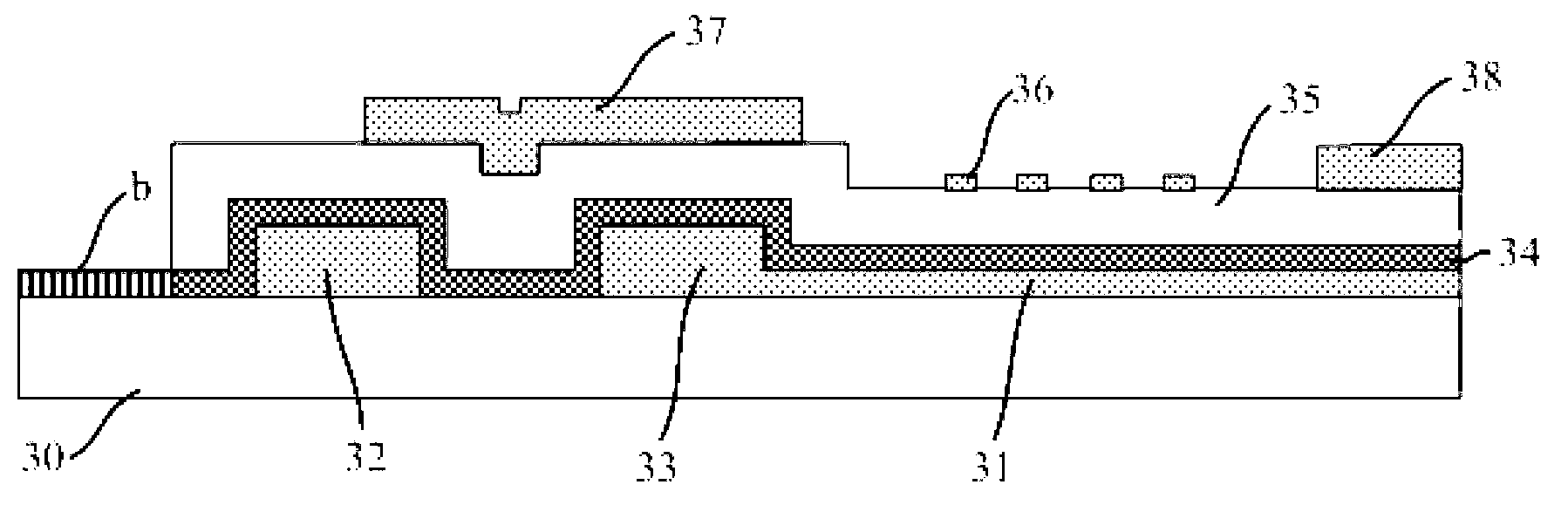
[0045] The array substrate of the embodiment of the present invention includes a plurality of pixel areas, and each pixel area includes:

[0046] A drain electrode, a source electrode, and a pixel electrode overlapping the drain electrode on the base substrate, wherein the pixel electrode is made of single-walled carbon nanotube material;

[0047] an active layer located on the drain electrode, the source electrode and the pixel electrode;

[0048] a gate insulating layer on the active layer; and

[0049] The gate on the gate insulating layer and the common electrode used to drive the liquid crystal to rotate, the common ...


PUM


Abstract

The invention relates to the field of manufacture of liquid crystal display devices, in particular to an array substrate and a manufacture method thereof, aiming to solve the problem that the traditional manufacture process of a TFT-LCD (Thin Film Transistor Liquid Crystal Display) based on an ADS (Advanced Super Dimension Switch) structure is complex and is low in efficiency. According to the embodiment of the invention, each pixel region of the array substrate comprises a drain electrode, a source electrode, a pixel electrode in lap joint with the drain electrode, an active layer located on the drain electrode, the source electrode and the pixel electrode, a grid insulating layer located on the active layer, a grid electrode and a public electrode, wherein the drain electrode and the source electrode are located on an underlayer substrate, the pixel electrode is made of a single-walled carbon nanotube material, the grid electrode and the public electrode are located on the grid insulating layer, and the public electrode has a slit-shaped structure. According to the embodiment of the invention, the array substrate can be prepared by adopting layout processes three times, so that the manufacture process is simplified, the manufacture efficiency is improved and the manufacture cost is reduced.

Description

technical field [0001] The invention relates to the field of manufacturing liquid crystal display devices, in particular to an array substrate and a manufacturing method thereof. Background technique [0002] Liquid Crystal Display (LCD) has the characteristics of small size, light weight, low power consumption, low radiation and low manufacturing cost, and has been widely used in various electronic devices, such as monitors, TVs, mobile phones, digital cameras, etc. digital electronics. Among them, TFT-LCD (Thin Film Transistor Liquid Crystal Display, Thin Film Transistor Liquid Crystal Display) is a main flat panel display device (FPD, Flat Panel Display). [0003] According to the direction of the electric field driving the liquid crystal, TFT-LCD is divided into vertical electric field type, horizontal electric field type and multi-dimensional electric field type. Among them, the vertical electric field type TFT-LCD needs to form pixel electrodes on the array substrate...

Claims


Application Information

Patent Timeline
Patent Type & Authority Applications(China)
IPC IPC(8): G02F1/1343G02F1/1362G02F1/1368H01L27/12H01L21/77
Inventor 杨静宁策
Owner BOE TECH GRP CO LTD
Why Eureka
Try Eureka