Array base plate, manufacturing method thereof and liquid crystal display device

A technology of array substrates and substrate substrates, which is applied in semiconductor/solid-state device manufacturing, optics, instruments, etc., and can solve problems such as large gate size, increased feed-in voltage ΔVp value, and increased TFT inter-electrode capacitance value, etc.

Inactive Publication Date: 2013-04-03
BOE TECH GRP CO LTD
View PDF6 Cites 23 Cited by
  • Summary
  • Abstract
  • Description
  • Claims
  • Application Information

AI Technical Summary

Problems solved by technology

[0007] Embodiments of the present invention provide an array substrate, a manufacturing method thereof, and a liquid crystal display device, which are used to solve the problem in the prior art that the TFT inter-electrode capacitance C is caused by the large gate size. gs and C gd The value of the increase leads to the problem that the value of the feed-in voltage ΔVp increases

Method used


Image

  • Array base plate, manufacturing method thereof and liquid crystal display device
  • Array base plate, manufacturing method thereof and liquid crystal display device
  • Array base plate, manufacturing method thereof and liquid crystal display device

Examples


Embodiment 1

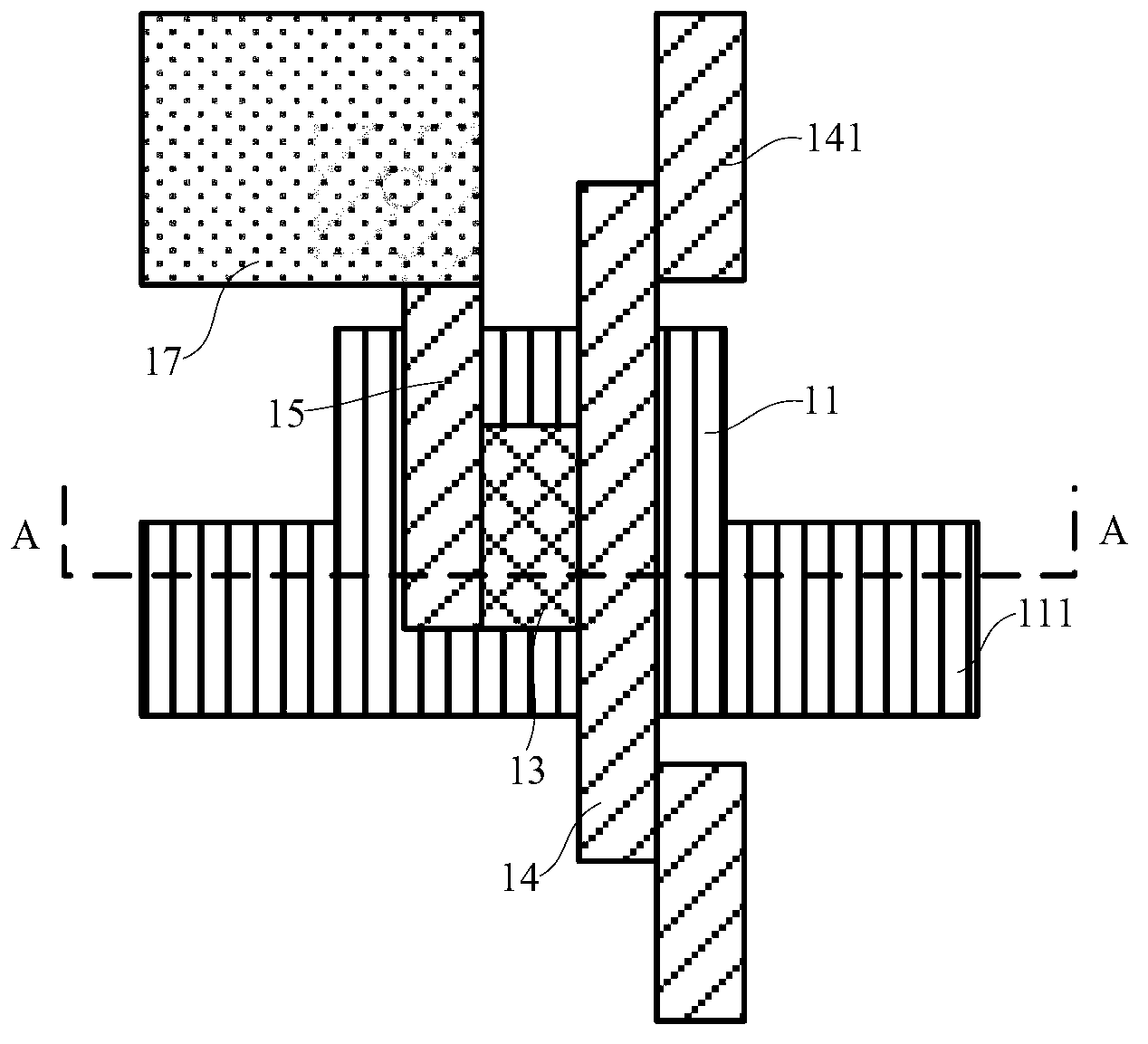
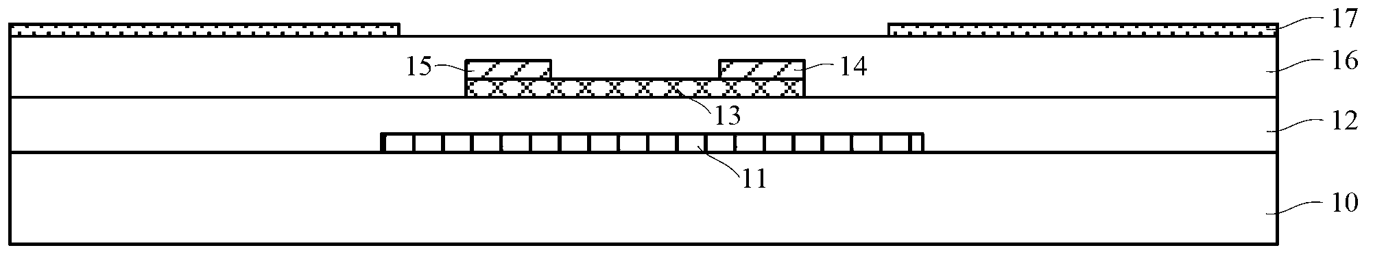
[0061] Embodiment 1. The structure of the array substrate in the embodiment of the present invention is as follows: Figure 3A and Figure 3B shown, where Figure 3B for Figure 3A The schematic diagram of the cross-sectional structure of the B-B direction of the array substrate shown, the array substrate of this embodiment includes:

[0062] substrate substrate 30;

[0063] The light-shielding layer 38 located on the base substrate 30 corresponding to the active layer 33, the light-shielding layer 38 is used to block the light entering the active layer 33 (that is, the light emitted from the backlight module), so that the active Layer 33 will not be exposed to light;

[0064] The grid 31 located on the light-shielding layer 38;

[0065] a gate insulating layer 32 on the gate 31;

[0066] an active layer 33 located on the gate insulating layer 32;

[0067] a source 34 and a drain 35 on the active layer 33;

[0068] A protection layer 36 located on the source electrode ...

Embodiment 2

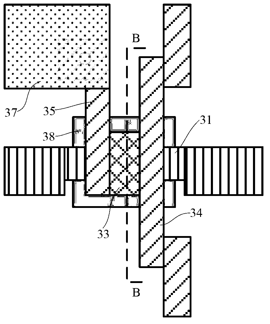
[0096] Embodiment 2. The structure of the array substrate in the embodiment of the present invention is as follows Figure 6A and Figure 6B As shown, among them, Figure 6B for Figure 6A The B-B direction sectional schematic diagram of the array substrate shown in this embodiment The array substrate includes:

[0097] substrate substrate 60;

[0098] A gate 61 located on the base substrate 60;

[0099] a gate insulating layer 62 on the gate 61;

[0100] A light-shielding layer 63 located on the gate insulating layer 62 and corresponding to the active layer 64, the light-shielding layer 63 is used to shield the light entering the active layer 64 (that is, the light emitted from the backlight module), so that there are The source layer 64 will not be irradiated by light;

[0101] The active layer 64 located on the light shielding layer 63;

[0102] a source 65 and a drain 66 on the active layer 64;

[0103] A protective layer 67 located on the source electrode 65 and the...

Embodiment 3

[0130] Embodiment 3. The structure of the array substrate in this embodiment is as follows: Figure 8A and Figure 8B As shown, among them, Figure 8B for Figure 8A The C-C direction sectional structure schematic diagram of the array substrate shown, the array substrate includes:

[0131] substrate substrate 800;

[0132] The light-shielding layer 801 and the pixel electrode 802 are located on the same layer on the base substrate 800, wherein the light-shielding layer 801 is located on the base substrate 800 at a position corresponding to the active layer 806, and is used to block light incident on the active layer 806 Light (that is, the light emitted from the backlight module), so that the active layer 806 will not be irradiated by light;

[0133] An insulating layer 803 located on the light-shielding layer 801, wherein the material of the insulating layer 803 can be silicon nitride or silicon oxide, etc.; the thickness of the insulating layer 803 is 200 nanometers to 1...


PUM

PropertyMeasurementUnit
thicknessaaaaaaaaaa
lengthaaaaaaaaaa

Abstract

The invention relates to the field of liquid crystal display and particularly relates to an array base plate, a manufacturing method thereof and a liquid crystal display device which are used for solving the problems of large grid electrode size and increased feed-in voltage value in the prior art. The array base plate provided by the embodiment of the invention comprises a thin film transistor arranged on a substrate base plate, a grid line connected with the thin film transistor and a shielding layer positioned between the substrate base layer and an active layer of the thin film transistor; the shielding layer is used for shielding light rays injected into the active layer; and the line width of a grid electrode is less than that of the grid line in which the grid electrode is positioned. According to the embodiment of the invention, the shielding layer shields the light rays injected into the active layer, and the line width of the grid electrode is less than that of the grid line in which the grid electrode is positioned, so that the value of the interelectrode capacitance of a TFT (Thin Film Transistor) is reduced, and further feed-in voltages influencing the frame level of a TFT-LCD (Liquid Crystal Display) can be reduced.

Description

technical field [0001] The invention relates to the field of liquid crystal display, in particular to an array substrate, a manufacturing method thereof, and a liquid crystal display device. Background technique [0002] Liquid Crystal Display (LCD) has the characteristics of low power consumption, low radiation and low manufacturing cost, and has been widely used in various electronic devices, such as digital electronic devices such as monitors, TVs, mobile phones, and digital cameras. Among them, a thin film transistor liquid crystal display (Thin Film Transistor Liquid Crystal Display, TFT-LCD) is a main flat panel display device (FPD, Flat Panel Display). [0003] Each pixel in the array substrate of the TFT-LCD is driven and controlled by a TFT element integrated on the array substrate and connected to the pixel. The structure of conventional TFT elements, such as figure 1 and figure 2 As shown, it includes: the gate 11 and the gate line 111 located on the base subs...

Claims


Application Information

Patent Timeline
Patent Type & Authority Applications(China)
IPC IPC(8): G02F1/1362G02F1/1368H01L21/77
Inventor 金熙哲刘圣烈崔承镇宋泳锡
Owner BOE TECH GRP CO LTD
Why Eureka
Try Eureka