
Method for manufacturing metal silicide thin film and ultra-shallow junction and semiconductor device

A technology of metal silicide and its manufacturing method, which is applied in semiconductor devices, semiconductor/solid-state device manufacturing, electrical components, etc., and can solve problems such as impurity diffusion

Inactive Publication Date: 2013-04-03
FUDAN UNIV
View PDF8 Cites 4 Cited by
  • Summary
  • Abstract
  • Description
  • Claims
  • Application Information

AI Technical Summary

Problems solved by technology

Due to the huge challenges of ultra-low energy ion implantation technology itself and the diffusion of impurities during annealing and activation, it is a huge challenge to use conventional ultra-low energy ion implantation and annealing activation technology to form field effect transistors suitable for future technology nodes.

Method used


Image

  • Method for manufacturing metal silicide thin film and ultra-shallow junction and semiconductor device
  • Method for manufacturing metal silicide thin film and ultra-shallow junction and semiconductor device
  • Method for manufacturing metal silicide thin film and ultra-shallow junction and semiconductor device

Examples


Embodiment Construction

[0021] In order to make the object, technical solution and advantages of the present invention clearer, various embodiments of the present invention will be described in detail below in conjunction with the accompanying drawings. However, those of ordinary skill in the art can understand that, in each implementation manner of the present invention, many technical details are provided for readers to better understand the present application. However, even without these technical details and various changes and modifications based on the following implementation modes, the technical solution claimed in each claim of the present application can be realized.

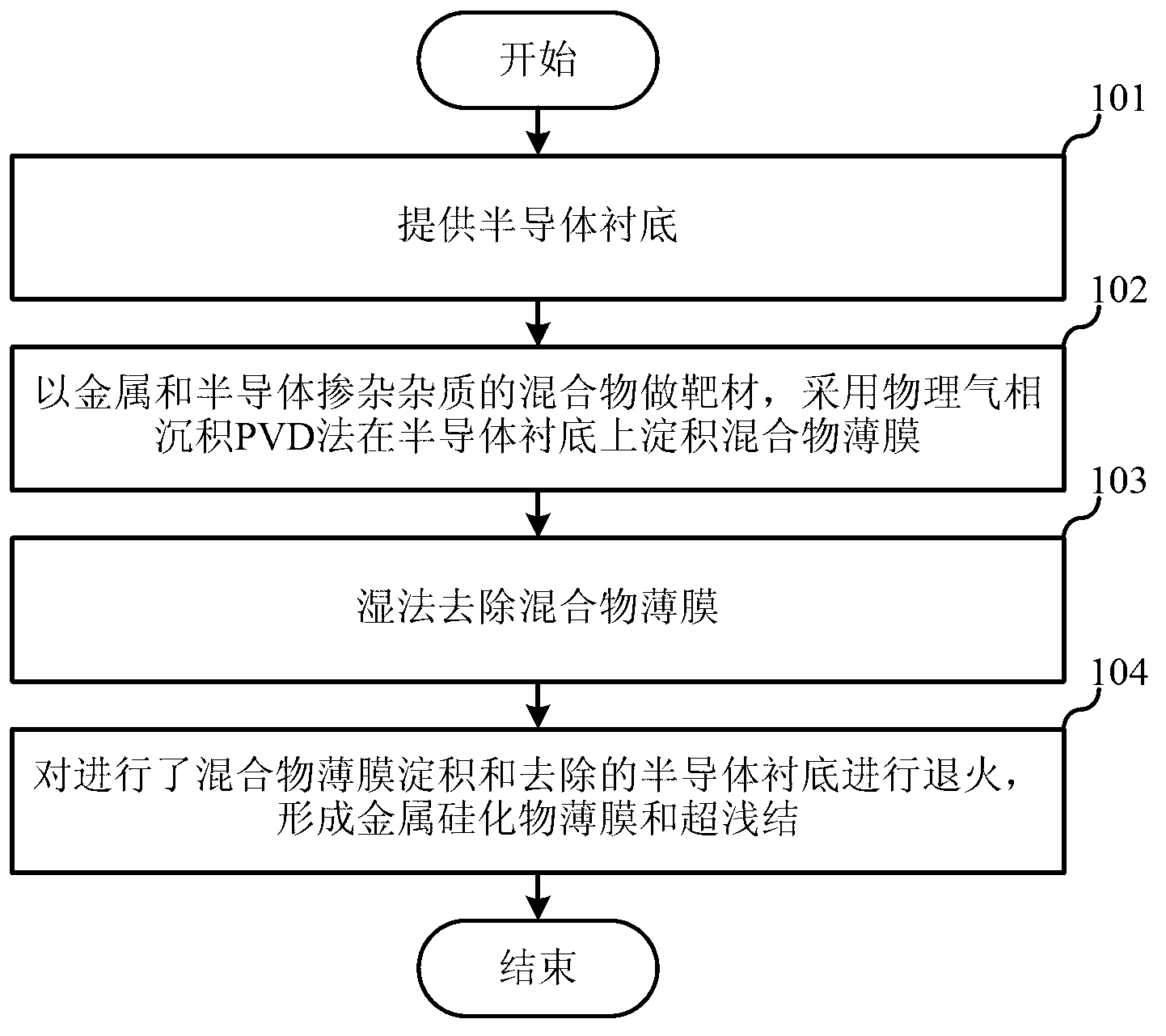
[0022] The first embodiment of the present invention relates to a method for fabricating a metal silicide thin film and an ultra-shallow junction. The specific process is as follows figure 1 shown, including the following steps:

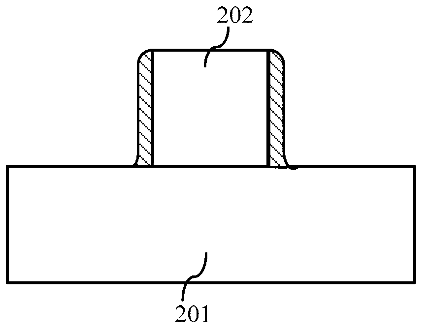
[0023] Step 101, providing a semiconductor substrate 201, such as Figure 2A Shown; the semic...


PUM


Abstract

The invention relates to the technical field of semiconductors and discloses a method for manufacturing a metal silicide thin film and an ultra-shallow junction and a semiconductor device. A mixture of metal and impurity doped semiconductor is used as a target material, a mixture thin film is deposited on a semiconductor substrate through a physical vapor deposition (PVD) method, the mixture thin film is removed by a wet process, and the annealing is performed to form the metal silicide thin film and the ultra-shallow junction. The mixture of metal and impurity doped semiconductor is used as the target material to deposit the mixture thin film, and the mixture thin film is removed by the wet process before heating and annealing, so that self limited ultra-thin uniform metal silicide thin film and ultra-shallow junction can be synchronously formed in the process of manufacturing a semiconductor field effect transistor, and the metal silicide thin film and the ultra-shallow junction can be applied to field effect transistors with 14nm, 11nm and below 11nm technology nodes.

Description

technical field [0001] The invention relates to the field of semiconductor technology, in particular to a method for making a metal silicide thin film and an ultra-shallow junction and a semiconductor device. Background technique [0002] With the advancement of the semiconductor industry, the feature size of semiconductor devices has become smaller and smaller with the innovation of process technology. While the lateral size of the device is continuously shrinking, the vertical size of the device is also shrinking accordingly. Especially when entering the node of 65 nanometers and below, the source / drain region and the source / drain extension region are required to be correspondingly shallower, and the doped junction with a junction depth below 100 nanometers is usually called an ultra-shallow junction (Ultra Shallow Junction, referred to as "USJ"), the ultra-shallow junction can better improve the short-channel effect of the device. As ultra-shallow junctions become shall...

Claims


Application Information

Patent Timeline
IPC IPC(8): H01L21/336H01L21/28H01L29/78
Inventor 吴东平许鹏张卫张世理
Owner FUDAN UNIV
Features
  • Generate Ideas
  • Intellectual Property
  • Life Sciences
  • Materials
  • Tech Scout
  • Unparalleled Data Quality
  • Higher Quality Content
  • 60% Fewer Hallucinations
Learn More