LED chip cutting method and LED chip manufactured by same

A technology of LED chip and cutting method, which is applied in semiconductor/solid-state device manufacturing, electrical components, circuits, etc., can solve problems such as unfavorable light extraction, and achieve the effect of improving light extraction efficiency

Inactive Publication Date: 2013-04-03
FOCUS LIGHTINGS SCI & TECH
View PDF4 Cites 13 Cited by
  • Summary
  • Abstract
  • Description
  • Claims
  • Application Information

AI Technical Summary

Problems solved by technology

[0002] Generally, after the introduction of sidewall corrosion in the sapphire substrate LED chip process, the wafer will be split directly af

Method used


Image

  • LED chip cutting method and LED chip manufactured by same
  • LED chip cutting method and LED chip manufactured by same

Examples


Example Embodiment

[0015] The preferred embodiments of the present invention will be described in detail below in conjunction with the accompanying drawings, so that the advantages and features of the present invention can be more easily understood by those skilled in the art, so as to define the protection scope of the present invention more clearly.

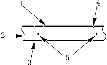
[0016] See attached figure 1 with attached figure 2 As shown, a method for cutting LED chips is provided in this implementation, including the following steps:

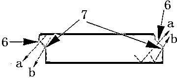
[0017] (1) Provide a sapphire substrate 2 with a GaN epitaxial light-emitting layer 1, perform laser scribing on the front side of the sapphire substrate 2 to form grooves 4 to divide the crystal grains, and use wet etching to etch the laser ablation area to form a groove in the groove Form a rough surface 7, according to the traditional chip manufacturing process, on this basis to complete the follow-up manufacturing of the chip;

[0018] (2) Thinning and polishing the sapphire subst...


PUM


Abstract

The invention discloses an LED chip cutting method on the basis of side-wall corrosion. The LED chip cutting method includes that an LED wafer is subjected to front laser scribing and side-wall corrosion and then is manufactured to form a chip according to a normal LED chip manufacturing process; back laser hidden cutting is carried out after the wafer is subjected to thinning and back plating, and positioning of hidden cutting lines is controlled, so that the hidden cutting lines are staggered from front scribing lines; and an oblique fracture surface is formed on each side wall of a crystal grain under the induction action of stress during fracturing, lateral light emergence is facilitated, the integral luminous flux of the chip is increased, and the appearance and the electric performance of the chip are unaffected. The invention further discloses the LED chip manufactured by the LED chip cutting method. Edges of the LED chip are in the shape of 'Z'-shaped sections with the oblique fracture surfaces. The 'Z'-shaped sections are manufactured by means of laser hidden cutting after the GaN wafer which is a semiconductor substrate is subjected to a chip side-wall corrosion process, accordingly, quantities of emergent light on the side walls are increased, and the brightness of the integral LED chip is improved.

Description

technical field [0001] The invention relates to the field of LED production and manufacturing, in particular to an LED chip cutting method. Background technique [0002] Usually, after the introduction of sidewall corrosion in the sapphire substrate LED chip process, the wafer will be split directly after the wafer is thinned. In this way, the sidewall of the produced chip will be relatively vertical, which is not conducive to side light emission. Contents of the invention [0003] The object of the present invention is to solve the problems in the prior art, and provide an LED chip cutting method which effectively increases the light output rate and the LED chip prepared therefrom. [0004] In order to achieve the above purpose, the present invention provides a LED chip cutting method based on sidewall etching, which includes the following steps: (1) providing a semiconductor substrate with a GaN epitaxial light-emitting layer, and performing laser scribing on the front s...

Claims


Application Information

Patent Timeline
IPC IPC(8): H01L33/00H01L21/78
Inventor 陈家洛陈立人
Owner FOCUS LIGHTINGS SCI & TECH
Why Eureka
Try Eureka