Wafer working tape

A wafer processing and adhesive technology, applied in the direction of film/sheet adhesive, adhesive type, electric solid device, etc., can solve the problem that the adhesive layer cannot be peeled off, and the adhesive layer is in contact with the adhesive layer Long time and other problems, to achieve the effect of full adhesion

Active Publication Date: 2013-04-03
FURUKAWA ELECTRIC CO LTD
View PDF8 Cites 6 Cited by
  • Summary
  • Abstract
  • Description
  • Claims
  • Application Information

AI Technical Summary

Problems solved by technology

[0003] For a wafer processing tape in which an adhesive layer and an adhesive layer are sequentially formed on a substrate in this way, the contact time between the adhesive layer and the adhesive layer must be long between manufacture and use. Therefore, the two layers are fused before use, and there is a problem that the adhesive layer cannot be peeled off smoothly from the adhesive layer in the process of picking up the singulated semiconductor element with the adhesive layer.

Method used


Image

  • Wafer working tape
  • Wafer working tape
  • Wafer working tape

Examples


Embodiment 1

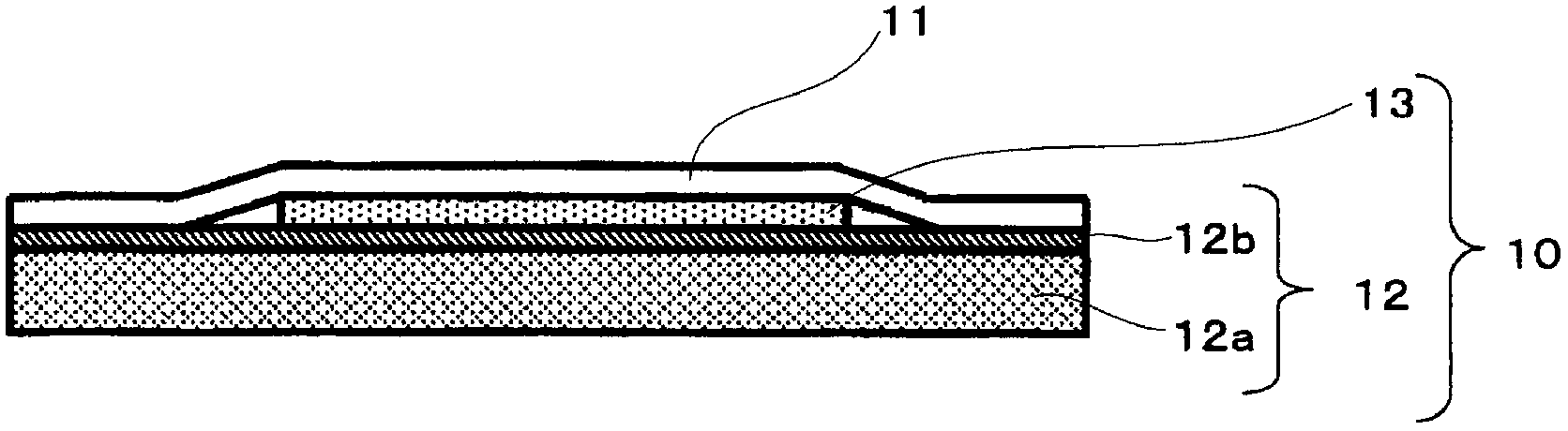
[0102] The adhesive layer (1) obtained above and the adhesive film (1) were bonded so that only one side of the PET film of the adhesive layer was peeled off, and the adhesive layer was in contact with the adhesive layer, and the supporting base material, the adhesive layer, and the Mixture layer, adhesive layer, anti-adhesive film, get figure 1 Wafer processing tape with release film shown. This wafer processing tape was used as a sample of Example 1.

Embodiment 2

[0104] The tape for wafer processing of Example 2 was produced by the method similar to Example 1 using the obtained said adhesive bond layer (2) and adhesive film (1).

Embodiment 3

[0106] The tape for wafer processing of Example 3 was produced by the method similar to Example 1 using the obtained said adhesive bond layer (3) and adhesive film (1).


PUM

PropertyMeasurementUnit
surface free energyaaaaaaaaaa
glass transition temperatureaaaaaaaaaa

Abstract

Provided is a wafer working tape wherein a support substrate, an adhesion layer, and a single binding layer are stacked in this order. The binding layer is used for pressure adhesion of a semiconductor element to either an external contact wiring member with wiring or another semiconductor element. The difference in surface free energy between the face of the binding layer which has detached from the adhesion layer and the face of the binding layer which is not in contact with the adhesion layer is 10 mJ / m2 or less.

Description

technical field [0001] The present invention relates to tapes for wafer processing. Background technique [0002] In the manufacturing process of semiconductor devices, the process of cutting (dicing) silicon wafers into chip units, picking up the cut semiconductor elements (chips), and then performing chip bonding on the picked up chips and lead frames and packaging substrates ( assembly) process. As a wafer processing tape used in the manufacturing process of the above-mentioned semiconductor device, a dicing tape in which an adhesive layer (temporary-adhesive layer) and an adhesive layer (adhesive layer) are sequentially formed on a support base material has been known in recent years. Die-bonding sheet (for example, see Patent Document 1). [0003] For a wafer processing tape in which an adhesive layer and an adhesive layer are sequentially formed on a substrate in this way, the contact time between the adhesive layer and the adhesive layer must be long between manufac...

Claims


Application Information

Patent Timeline
Patent Type & Authority Applications(China)
IPC IPC(8): H01L21/301C09J7/02C09J133/20C09J201/00
CPCH01L21/6836H01L2221/68377H01L2221/68327H01L21/683C09J2203/326C09J7/385C09J7/22C09J2301/302C09J2301/312
Inventor 青山真沙美石渡伸一矢吹朗石黑邦彦铃木俊宏
Owner FURUKAWA ELECTRIC CO LTD
Why Eureka
Try Eureka