
Manufacturing method of touch panel

A manufacturing method and touch panel technology, applied in the input/output process of data processing, instruments, electrical digital data processing, etc., can solve the problem of increasing the cost of manufacturing materials and time, and the inability to effectively solve the problem of the reflection of the wire layer 2 and the inability of the light-shielding layer Completely cover the wire layer 2 and other issues to achieve the effect of reducing the amount of reflected light

Inactive Publication Date: 2013-04-10
CANDO
View PDF4 Cites 6 Cited by
  • Summary
  • Abstract
  • Description
  • Claims
  • Application Information

AI Technical Summary

Problems solved by technology

[0008] As far as production is concerned, the biggest problem of such production is that the exposure process must be precisely aligned relative to the wire layer 2 using the same photomask with the touch image. As long as the alignment is not good, the formed light shielding layer will not be completely Covering the wire layer 2 cannot effectively solve the problem of light reflection generated by the wire layer 2. In addition, in order to reduce the light reflection, the manufacturing steps of coating photoresist, mask alignment, exposure, development, and etching are repeated to form light shielding. The process of layering also increases the cost of production materials and time

Method used


Image

  • Manufacturing method of touch panel
  • Manufacturing method of touch panel
  • Manufacturing method of touch panel

Examples


Embodiment Construction

[0032] Below in conjunction with accompanying drawing and embodiment, the present invention is described in detail:

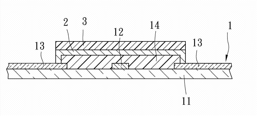
[0033] see Figure 4 , the touch panel made by a preferred embodiment of the manufacturing method of the touch panel of the present invention is as follows figure 1 , 3 Shown includes a substrate 1 , a wire layer 2 formed on the surface of the substrate 1 , and a light shielding layer 3 formed on the wire layer 2 away from the surface of the substrate 1 .

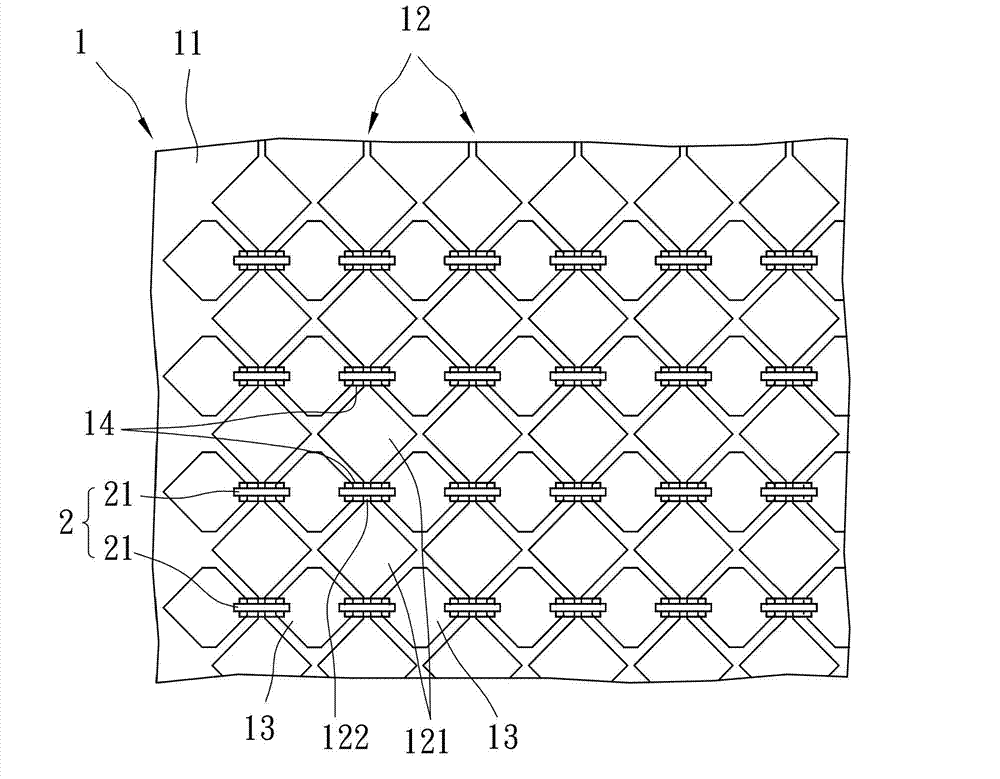
[0034] see figure 1 , image 3 , the substrate 1 has a base material 11, a plurality of first transparent conductive films 12 formed on the surface of the base material 11 in strips and arranged in rows, a plurality of second transparent conductive films 13, and a plurality of The insulating film 14 on the first transparent conductive film 12 .

[0035] More specifically, the base material 11 on the substrate 1 is a flexible plastic soft board or a thin sheet of transparent glass. The first and second ...


PUM


Abstract

A manufacturing method of a touch panel is to form a conducting line layer showing a touch pattern on a substrate, and comprises the following steps: (a) forming a conducting line preparation layer by using conducting materials on the substrate; (b) coating a shading preparation layer formed by a material with reflectivity lower than the conducting line preparation layer on the conducting line preparation layer; (c) forming a shading layer from the shading preparation layer through exposure and development by using a shade with the touch pattern; and (d) etching the conducting line preparation layer by using the shading layer as a shade for the conducting line preparation layer to remove areas not shaded on the conducting line preparation layer, so as to obtain the conducting line layer with the touch pattern. The invention performs etching manufacturing only by using lithography once and using the formed shading layer for self-alignment to form the conducting line layer and the shading layer without position errors, which improves process yield, reduces manufacturing material cost and manufacturing time cost.

Description

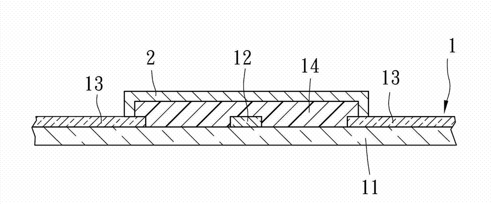
technical field [0001] The present invention relates to a manufacturing method of a panel, in particular to a manufacturing method of a touch panel. Background technique [0002] see figure 1 and figure 2 , a general touch panel includes a substrate 1 and a layer of conductor layers 2 . [0003] The substrate 1 includes a substrate 11 , a plurality of first transparent conductive films 12 and second transparent conductive films 13 formed on the substrate 11 with a predetermined pattern and mainly made of indium tin oxide, and a plurality of The insulating material constitutes and forms a sheet and correspondingly forms the insulating film 14 on the surface of the first transparent conductive film 12 . [0004] The wire layer 2 has a plurality of conductive film blocks 21 formed on the insulating layer to form a touch pattern, and each conductive film block 21 is correspondingly formed on each insulating film 14 and extends outward to be the same as the most The adjacent...

Claims


Application Information

Patent Timeline
Patent Type & Authority Applications(China)
IPC IPC(8): G06F3/041
Inventor 李文政林钟伟薛秉中庄恒隆赖纪光
Owner CANDO
Learn More