Method for precisely controlling thinning of wafer

A technology of precise control and thin thickness, applied in semiconductor/solid-state device manufacturing, electrical components, circuits, etc., can solve problems such as unsatisfactory and unsatisfactory thickness control accuracy

Active Publication Date: 2013-04-10
SHANGHAI HUAHONG GRACE SEMICON MFG CORP
View PDF4 Cites 16 Cited by
  • Summary
  • Abstract
  • Description
  • Claims
  • Application Information

AI Technical Summary

Problems solved by technology

The elasticity of the blue film material also has a great influence on the thinning thickness of the wafer, which makes the accuracy of thickness control even more unsatisfactory. With the rapid development of technology, this accuracy can no longer meet the needs of some products.

Method used


Image

  • Method for precisely controlling thinning of wafer
  • Method for precisely controlling thinning of wafer
  • Method for precisely controlling thinning of wafer

Examples


example 1

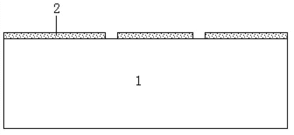
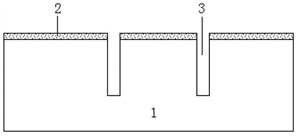
[0055] 1) Coat a layer of 4 micron photoresist 2 on the silicon wafer 1, and form a groove 3 pattern (such as a rectangle) at the cutting line.

[0056] 2) Using the plasma silicon etching method, the pattern of the trench 3 on the scribe line is etched to a specified thinning thickness of 15 microns (that is, the depth of the trench 3 is 15 microns).

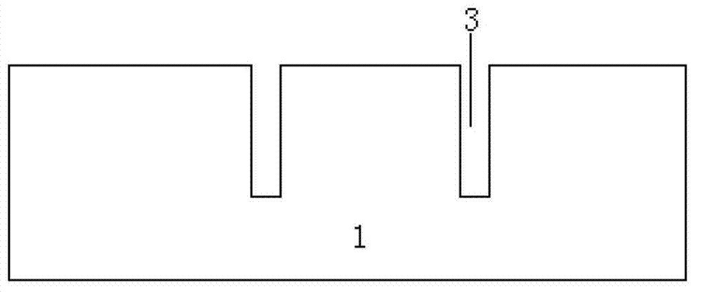
[0057] 3) A photoresist ashing machine is used to remove the photoresist 2 on the surface of the silicon wafer 1 .

[0058] 4) The groove 3 is filled with tungsten by using a low-pressure chemical vapor deposition method.

[0059] 5) Complete the wafer process.

[0060] 6) Paste the blue film on the front of the wafer.

[0061] 7) The wafer is thinned to the bottom of the groove by Taikoo, and the thinning machine is controlled to stop on the tungsten at the bottom of the groove 3 by means of current rise.

[0062] 8) Peel off the front blue film, and the wafer thinning is completed.

[0063] The advantage of wafer thinning a...


PUM


Abstract

The invention discloses a method for precisely controlling thinning of a wafer. The method for precisely controlling thinning of the wafer includes that a step of etching of a silicon wafer groove is added in a chip machining process, fillers are arranged in the groove, after the machining process of a front-side chip of a wafer is completed, the back side of the silicon wafer is thinned to the bottom of the groove, and precision control of wafer thinning is achieved. The method for precisely controlling thinning of the wafer can precisely control the thinning of the wafer, differences of thickness among wafers are reduced, and influence of the thickness of a blue film on thinning precision is prevented.

Description

technical field [0001] The invention relates to a wafer thinning method in the semiconductor field, in particular to a method for precisely controlling the wafer thinning thickness. Background technique [0002] With the development of semiconductor technology, 3D packaging technology has increasingly become a key technology for the core competition of major companies. With the application and promotion of 3D technology, the demand for the thickness of the wafer is getting higher and higher. At present, the world's thinnest thickness is 10 microns. [0003] With the current wafer thinning technology, the in-plane accuracy range is controlled at 2.5 microns, and the wafer-to-wafer accuracy range is controlled at 6 microns. The elasticity of the blue film material also has a great influence on the thinning thickness of the wafer, which makes the accuracy of thickness control even more unsatisfactory. With the rapid development of technology, this accuracy can no longer meet ...

Claims


Application Information

Patent Timeline
Patent Type & Authority Applications(China)
IPC IPC(8): H01L21/02
Inventor 郁新举
Owner SHANGHAI HUAHONG GRACE SEMICON MFG CORP
Why Eureka
Try Eureka