Vertical transition structure among three-dimensional multi-chip component boards

A multi-chip component and vertical transition technology, which is applied in the direction of electrical components, electric solid-state devices, semiconductor devices, etc., can solve the problem of occupying laminated circuit boards, side circuits and horizontal circuits with high process requirements and restricting the density of chip components and assembly efficiency to achieve the effect of ensuring realizability and alleviating the strict requirements of alignment accuracy

Inactive Publication Date: 2013-04-10
SOUTHEAST UNIV
View PDF3 Cites 5 Cited by
  • Summary
  • Abstract
  • Description
  • Claims
  • Application Information

AI Technical Summary

Problems solved by technology

Its interconnection technologies currently include: wire bonding (or TAB) vertical interconnection technology, thin film metallization vertical interconnection technology, bump (or solder ball) vertical interconnection technology, isolation plate through-hole metallization vertical interconnection technology, etc. However, these technologies are all interconnection technologies made on laminated circuit boards, which need to occupy the area of ​​laminated...

Method used


Image

  • Vertical transition structure among three-dimensional multi-chip component boards

Examples


Embodiment Construction

[0015] The present invention will be further described below in conjunction with drawings and embodiments.

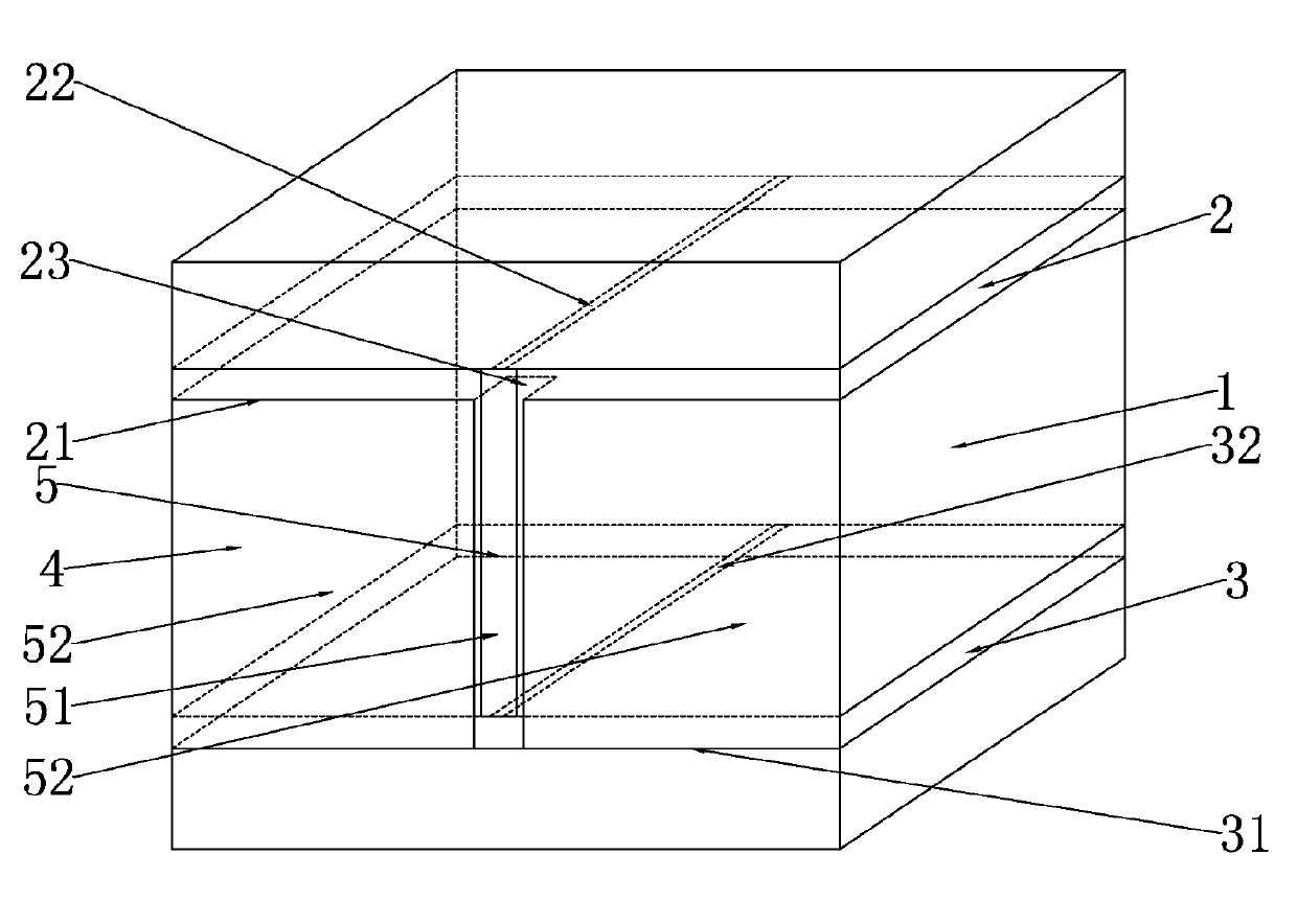
[0016] The vertical transition structure between the three-dimensional multi-chip component boards of the present invention is specifically as follows: the upper layer circuit board 2 and the lower layer circuit board 3 are stacked and packaged in the three-dimensional component module 1, and the upper layer circuit board 2 has an upper layer microstrip line conduction belt 22, The lower layer circuit board 3 has a lower layer of microstrip line conduction tape 32, and the upper layer of microstrip line conduction tape 22 and the lower layer of microstrip line conduction tape 32 are all to the edges of the circuit boards 2 and 3 to ensure that the upper layer of microstrip line conduction tape 22 and the lower microstrip line conduction strip 32 can be well connected with the side surface circuit; the side surface of the three-dimensional component module 1 adopts a copl...


PUM


Abstract

The invention discloses a transition structure among three-dimensional multi-chip component boards. The transition structure among the three-dimensional multi-chip component boards comprises a three-dimensional component module made of epoxy resin, an upper-layer circuit board sealed in the three-dimensional component module and a lower-layer circuit board sealed in the three-dimensional component module, a metal layer laid on the surface of the three-dimensional component module and a coplanar waveguide sculptured on the metal layer. The upper-layer circuit board is arranged under the lower-layer circuit board in a paralleled mode, and the coplanar waveguide is vertically arranged on the lateral side of the three-dimensional component module and is perpendicular to the upper-layer circuit board and the lower-layer circuit board. The transition structure among the three-dimensional multi-chip component boards is capable of conducting a three-dimensional vertical interconnection on a lateral side of a 3D-Multi Chip Module (MCM), and achieving vertical interconnections among multi-layer circuit boards. Areas of planar circuits are not occupied by the interconnections. Signal transmission has a wide frequency band, little insertion loss, little return loss and a simple structure. Circuit functions of expanding filtering and distributing power and the like are easy to expand on the interconnections arranged on the lateral side. Further, requirements to registration precision of a vertical circuit and a horizontal circuit are not high, accordingly technical implementability is high.

Description

technical field [0001] The invention relates to a vertical transition structure, in particular to a vertical transition structure between three-dimensional multi-chip component boards. Background technique [0002] Three-dimensional multi-chip module (3D-MCM) is a multi-chip module technology developed on the basis of two-dimensional multi-chip module (2D-MCM) technology. Among the 3D-MCMs, stacked 3D-MCM is currently the most widely used one. Its interconnection technologies currently include: wire bonding (or TAB) vertical interconnection technology, thin film metallization vertical interconnection technology, bump (or solder ball) vertical interconnection technology, isolation plate through-hole metallization vertical interconnection technology, etc. However, these technologies are all interconnection technologies made on laminated circuit boards, which need to occupy the area of ​​laminated circuit boards, which restricts the density and assembly efficiency of circuit m...

Claims


Application Information

Patent Timeline
IPC IPC(8): H01L23/538
Inventor 王磊殷晓星赵洪新
Owner SOUTHEAST UNIV
Why Eureka
Try Eureka