Patterned substrate and light emitting diode (LED) chip used for LED inverted-assembly structure

A patterned substrate and flip-chip technology, applied in electrical components, circuits, semiconductor devices, etc., can solve the problems of hemispherical pattern parameter selection that has not yet formed a system, and achieve improved internal quantum efficiency, luminous flux, and improved luminous flux. The effect of light extraction efficiency

Inactive Publication Date: 2013-04-10
SOUTH CHINA UNIV OF TECH
View PDF5 Cites 0 Cited by
  • Summary
  • Abstract
  • Description
  • Claims
  • Application Information

AI Technical Summary

Problems solved by technology

[0006] Even though hemispherical patterned substrates have greatly improved the light extraction efficiency of LEDs, most of the current applications of hemispherical patterned substrates in LED chips use positive mounting structures; researchers also lack parameters for hemispherical patterns (including bottom radius and edge distance) to carry out a systematic discussion, the selection of hemispherical pattern parameters has not yet formed a systematic system

Method used


Image

  • Patterned substrate and light emitting diode (LED) chip used for LED inverted-assembly structure
  • Patterned substrate and light emitting diode (LED) chip used for LED inverted-assembly structure
  • Patterned substrate and light emitting diode (LED) chip used for LED inverted-assembly structure

Examples


Embodiment 1

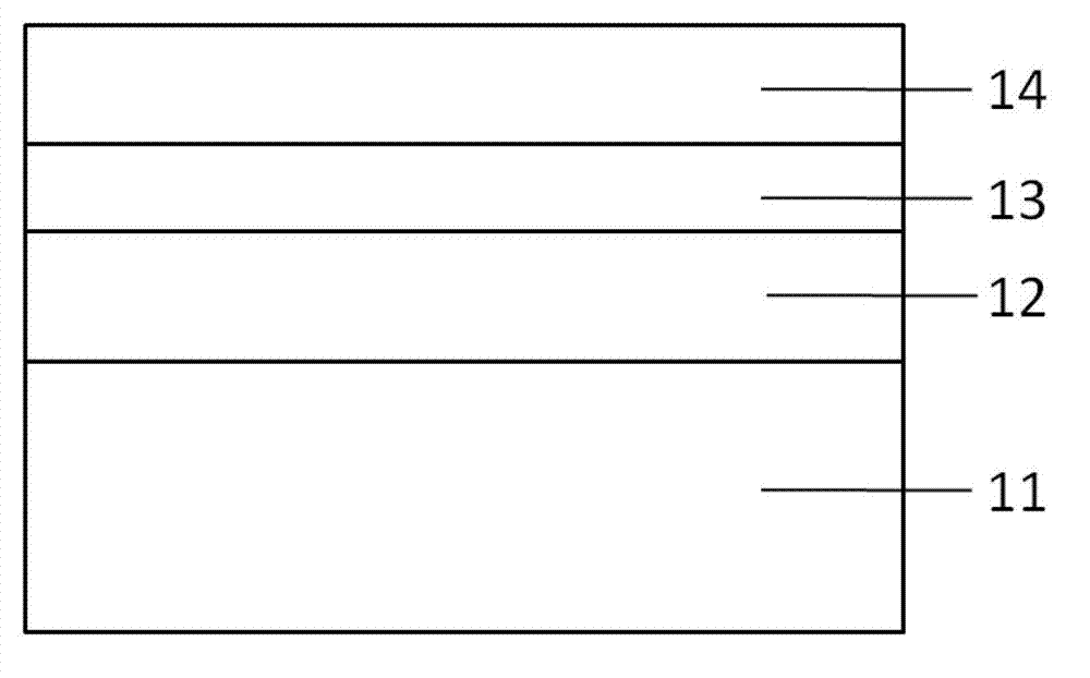
[0030] figure 1 Be the schematic diagram of the LED chip of this embodiment, as figure 1 As shown, it consists of a patterned sapphire substrate 11, an N-type GaN layer 12, an MQW quantum well layer 13, and a P-type GaN layer 14 arranged in sequence.

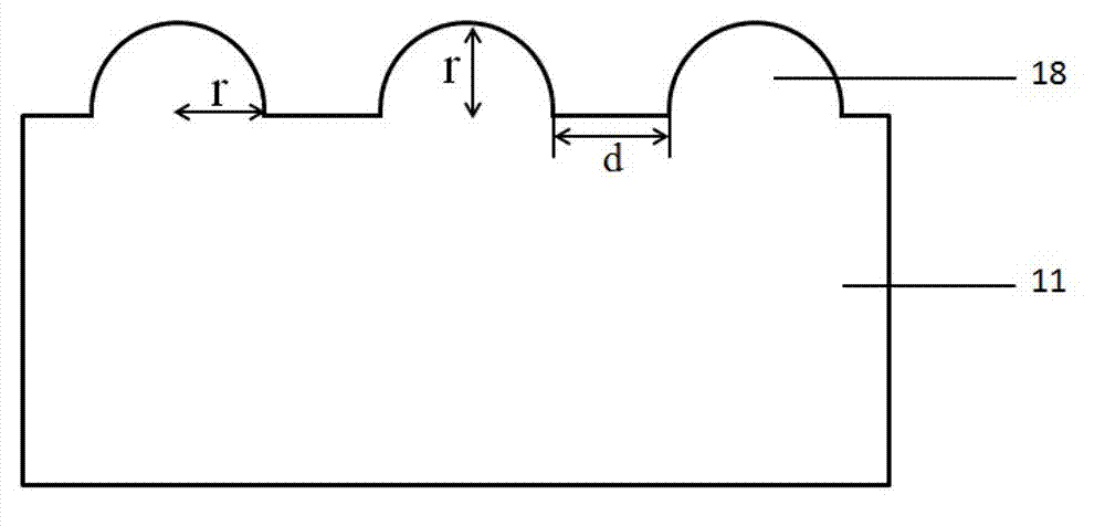
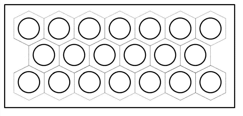
[0031] like figure 2 As shown, in the patterned substrate of the LED chip of the present embodiment, the pattern of the substrate is composed of a plurality of hemispheres 18 of the same shape arranged on the surface of the substrate; the height of the hemisphere is equal to the radius r of the bottom surface of the corresponding hemisphere; the adjacent hemisphere The edge spacing d is 0.7 times of the radius r of the bottom surface of the hemisphere; the radius r of the bottom surface of the hemisphere is 2 μm in the present embodiment; image 3 The hexagonal arrangement shown.

[0032] Figure 4 It is a schematic diagram of applying the patterned substrate to the LED flip-chip structure in this embodiment. Each layer in...

Embodiment 2

[0034] The patterned substrate of the LED chip of the present embodiment has a refractive index of 1.1, and the pattern of the substrate is composed of a plurality of hemispheres of the same shape arranged on the surface of the substrate; the height of the hemisphere and the radius r of the bottom surface of the corresponding hemisphere Equal; the edge spacing d of adjacent hemispheres is 0.9 times of the base radius r of the hemisphere; the base radius r of the hemisphere is 2.8 μ m in the present embodiment; Figure 5 The rectangular arrangement shown.

Embodiment 3

[0036] The patterned substrate of the LED chip of the present embodiment has a refractive index of 2, and the pattern of the substrate is composed of a plurality of hemispheres of the same shape arranged on the surface of the substrate; the height of each hemisphere is the same as the bottom surface of the corresponding hemisphere The radii r are equal; the distance d between the edges of adjacent hemispheres is 1.0 times the radius of the bottom surface of the hemisphere; the radius r of the bottom surface of the hemisphere in this embodiment is 3.0 μm; the multiple hemispheres with the same shape are arranged in a rectangular manner.


PUM


Abstract

The invention discloses a patterned substrate and a light emitting diode (LED) chip used for an LED inverted-assembly structure. Patterns of the substrate are formed by a plurality of semispheres in the same shape and arranged on the surface of the substrate, the height of each semisphere is the same as a bottom surface radius r of a corresponding semisphere, and the distance d between adjacent semispheres is 0.7-1.0 times of the bottom surface radius r of each semisphere. Compared with the prior art, light emission advantages of the semispheric patterns are fully taken, the luminous flux of the patterned substrate and the LED chip used for the LED inverted-assembly structure is improved for 6-11% compared with the patterned substrate and the LED chip used for an LED forward-assembly structure, and processing and popularization are convenient.

Description

technical field [0001] The invention relates to an LED chip, in particular to a patterned substrate for an LED flip-chip structure and an LED chip. Background technique [0002] Patterned substrate technology is a recent research hotspot in the field of GaN-based LEDs on sapphire substrates. Since its pattern evolution, it has significantly improved the LED light extraction effect and epitaxy quality, and has become an important way to improve LED performance. [0003] The improvement of the optical performance of the LED by the substrate pattern is reflected in two aspects: on the one hand, the pattern changes the trajectory of the light through scattering / reflection, so that the incident angle of the light exiting at the interface becomes smaller (less than the critical angle of total reflection), and then it is transmitted out. Improve the light extraction rate; on the other hand, the pattern can also make the subsequent GaN growth appear the effect of lateral epitaxy, r...

Claims


Application Information

Patent Timeline
IPC IPC(8): H01L33/20
Inventor 李国强周仕忠林志霆王海燕
Owner SOUTH CHINA UNIV OF TECH
Why Eureka
Try Eureka