Structure and manufacturing method of semiconductor device

A device structure and semiconductor technology, used in semiconductor devices, electrical solid devices, electrical components, etc., can solve the problems of unsatisfactory varistor characteristics and low resistance in high resistance states.

Inactive Publication Date: 2013-04-10
SHANGHAI HUAHONG GRACE SEMICON MFG CORP
View PDF4 Cites 6 Cited by
  • Summary
  • Abstract
  • Description
  • Claims
  • Application Information

AI Technical Summary

Problems solved by technology

[0002] see figure 1 As shown, the existing semiconductor device structure using titanium nitride as the upper electrode, its resistance characteristics show that the initial resistance is very small, only tens of ohms ( figure 1 The display is only 35 ohms), the resistance of the low resistance state is only about 200 ohms; the rheostatic performance is not ideal, and the resistance of the high resistance state decreases significantly with the increase of the number of erasing and writing

Method used


Image

  • Structure and manufacturing method of semiconductor device
  • Structure and manufacturing method of semiconductor device
  • Structure and manufacturing method of semiconductor device

Examples


Embodiment Construction

[0022] The manufacturing process method of the semiconductor device, comprising the steps of:

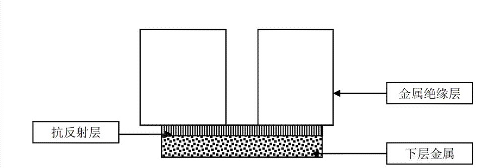
[0023] Step 1, see image 3 As shown, the lower metal layer, the anti-reflection layer and the metal insulating layer are sequentially formed from bottom to top.

[0024] Step 2. A through hole may be formed in the metal insulating layer by using various known techniques.

[0025] Step three, see Figure 4 As shown, a layer of metal is deposited on the sidewall of the via hole as a barrier layer. The metal material of the barrier layer includes but not limited to titanium nitride.

[0026] Step 4, see Figure 5 As shown, metal is deposited in the through hole and completely filled to serve as the bottom electrode; the metal material of the bottom electrode includes but not limited to metal tungsten.

[0027] Step five, see Figure 6 As shown, rapid thermal oxidation (RTO) is used to oxidize the metal on the upper part of the through hole to form a metal oxide layer on the uppe...


PUM


Abstract

The invention discloses a structure of semiconductor device. The structure of the semiconductor device comprises a medal mounted on a lower layer, an anti-reflection layer and a medal insulator formed in sequence on the upper surface of the medal mounted on the lower layer. Medal as a lower electrode is deposited in a through-hole of the medal insulator and a medal oxide layer is formed on the upper end of the lower electrode. A barrier layer made of medals is arranged among the lower electrode, the medal oxide layer, and the side wall of the through-hole. The structure of the semiconductor device is characterized in that a medal aluminum layer deposited on the upper end of the medal insulator and the upper end of the medal oxide layer is further included, the medal aluminum layer is an upper electrode, and medal-insulator-medal is finally formed by the lower electrode, the medal oxide layer, and the medal aluminum layer. The invention further discloses a manufacturing method of semiconductor. Initial resistance can be significantly improved, and the structure and manufacturing method of the semiconductor device has good characteristics of variable resistance.

Description

technical field [0001] The invention relates to the field of semiconductor integrated circuits, in particular to a semiconductor device structure. The invention also relates to a manufacturing process method of the semiconductor device structure. Background technique [0002] see figure 1 As shown, the existing semiconductor device structure using titanium nitride as the upper electrode, its resistance characteristics show that the initial resistance is very small, only tens of ohms ( figure 1 The display is only 35 ohms), and the resistance of the low-resistance state is only about 200 ohms; the performance of the varistor characteristics is not ideal, and the resistance of the high-resistance state decreases significantly as the number of erasing and writing increases. Contents of the invention [0003] The technical problem to be solved by the present invention is to provide a semiconductor device structure, which can significantly increase the resistance value of the...

Claims


Application Information

Patent Timeline
Patent Type & Authority Applications(China)
IPC IPC(8): H01L45/00H01L27/24
Inventor 成鑫华许升高
Owner SHANGHAI HUAHONG GRACE SEMICON MFG CORP
Why Eureka
Try Eureka