Method for forming shallow junction

A shallow junction and integrated circuit technology, applied in the field of forming drain-source shallow junctions, can solve problems such as elimination, and achieve the effects of stable distribution of impurity concentration, reduction of processes, and easy control of junction depth.

Inactive Publication Date: 2002-12-18
SHANGHAI INTEGRATED CIRCUIT RES & DEV CENT +1
View PDF0 Cites 1 Cited by
  • Summary
  • Abstract
  • Description
  • Claims
  • Application Information

AI Technical Summary

Problems solved by technology

However, the use of silicide itself as a diffusion source here has certain problems in the control of impurity distribution and process repeatability, and the diffusion process itself has been eliminated in advanced manufacturing processes.

Method used


Image

  • Method for forming shallow junction
  • Method for forming shallow junction

Examples


Embodiment Construction

[0021] Implementation steps of the present invention are as follows:

[0022] 1. Clean the wafer surface with diluted hydrofluoric acid

[0023] 2. Deposit the metal required to form silicide on the surface of the silicon wafer by PVD method, such as Co (cobalt) / Ti (titanium)

[0024] 3. Using rapid thermal annealing method, at a lower temperature, such as 550 degrees, to form a high-resistance silicide, such as CoSi

[0025] 4. Corrosion away unnecessary and unreacted metals, such as Co or Ti metals.

[0026] 5. Through rapid thermal annealing at a higher temperature, such as 850 degrees, to form a low-resistance silicide, such as CoSi 2

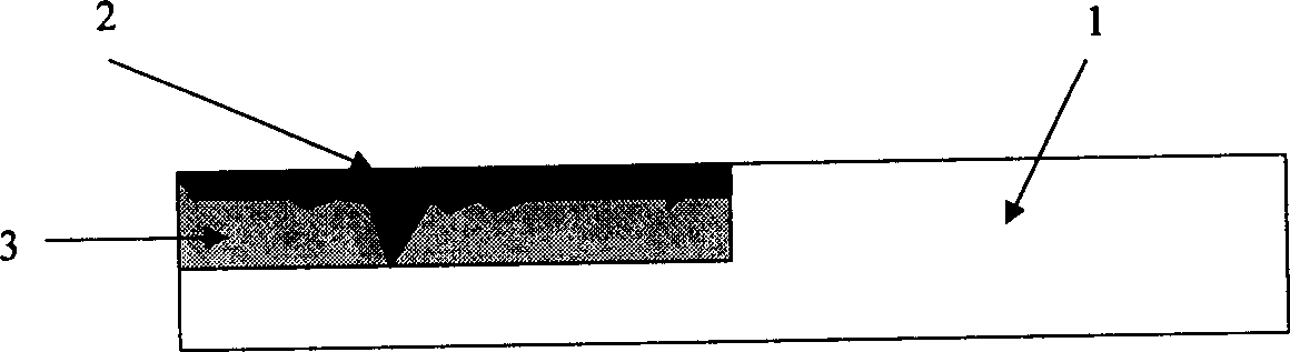
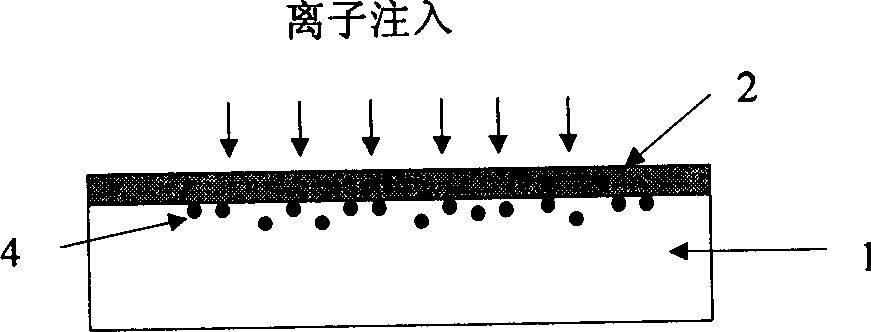
[0027] 6. Using silicide as an implant mask, such as CoSi 2 , to complete the implantation of the source / drain junction and the gate dose, the peak of the impurity concentration is just below the silicide, such as about 5nm

[0028] 7. Use SPIKE annealing or IMPULSE annealing to form a shallow junction.

[0029] The shallow junction p...


PUM


Abstract

Present silicide is prepared after insert source/drain and anneal excited to form junctions with the reliability problem mainly on electric drain which influences the final performance of transistors. This ivnention is to form silicide first, then inject in impurities and anneal to junction. The distributed peak value of inserted impurities lies under the silicide avoiding the problem brought with the diffusion of silicide in which the junction is easy to be controlled, high impurities concentration and repeatability, reducing the procedure of taking oxide as the injection mask.

Description

technical field [0001] The invention belongs to the technical field of integrated circuit manufacturing technology, and in particular relates to a method for forming a drain-source shallow junction. Background technique [0002] With the continuous development of integrated circuits, the minimum line width of transistors continues to shrink. The current mainstream technology of 0.18um technology means that the length of the gate is 0.18 microns. While the line width is continuously shrinking, in order to improve the performance of the transistor, the depth of the source / drain junction is also continuously reduced. The depth of the junction is only tens of nanometers in the 0.18μm process. [0003] The current mainstream process is to grow silicide after the source / drain junction of the transistor is defined, that is, after the high-dose implantation and annealing of the junction are completed. Since the growth of the silicide itself will consume part of the silicon, if the ...

Claims


Application Information

Patent Timeline
Patent Type & Authority Applications(China)
IPC IPC(8): H01L21/265H01L21/324
Inventor 胡恒升
Owner SHANGHAI INTEGRATED CIRCUIT RES & DEV CENT
Why Eureka
Try Eureka