Method to thin a silicon-on-insulator substrate

Active Publication Date: 2015-02-24
S O I TEC SILICON ON INSULATOR THECHNOLOGIES
View PDF12 Cites 2 Cited by
  • Summary
  • Abstract
  • Description
  • Claims
  • Application Information

AI Technical Summary

Benefits of technology

[0021]One particular objective of the invention is to provide a method allowing thinning of the active surface layer of an initial substrate of SOI type, whilst eliminating the

Problems solved by technology

When it is desired to thin the active silicon surface layer of the substrate, notably by etching, it is ascertained that the edges of the wafers are fragile, that they may break and form particles that are re-deposited on the active layer, thereby polluting this layer.
However, the applicant has found that when the active silicon layer is considerably thinned, the so-called “encapsulation” layer, i.e., the layer facing the peripheral edge of the buried oxide, becomes dama

Method used


Image

  • Method to thin a silicon-on-insulator substrate
  • Method to thin a silicon-on-insulator substrate
  • Method to thin a silicon-on-insulator substrate

Examples


Embodiment Construction

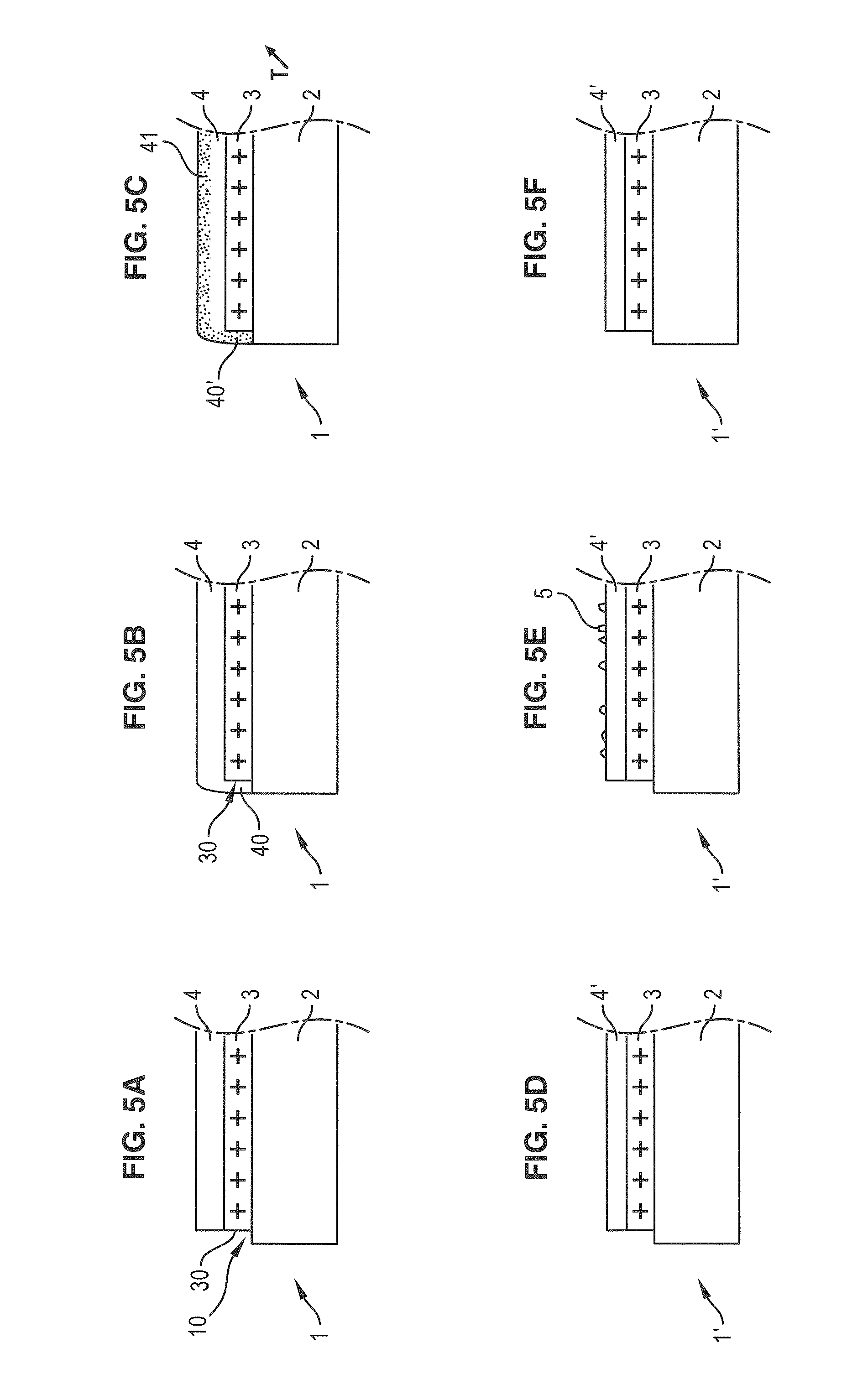
[0042]The method according to the invention will now be described.

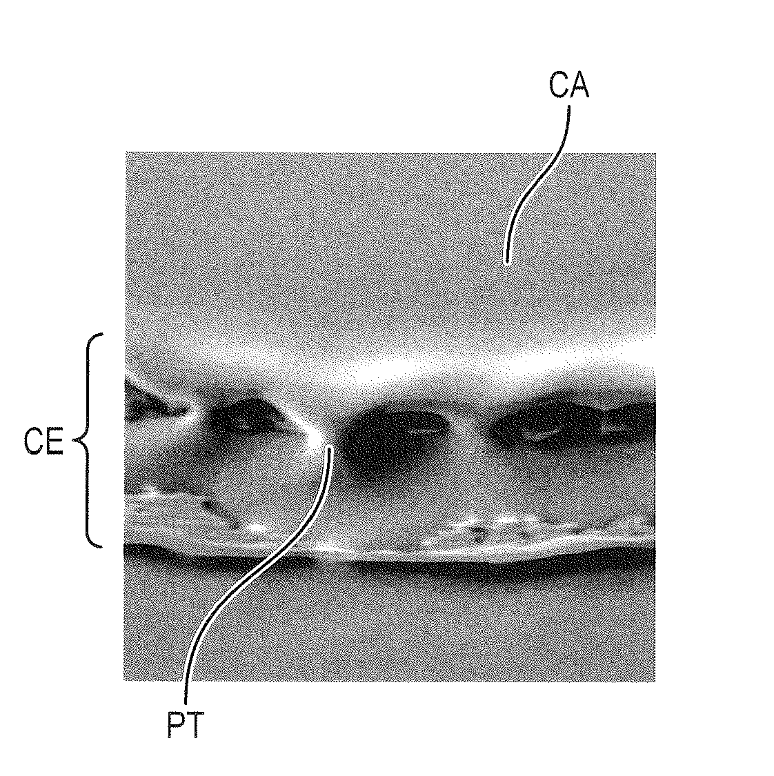
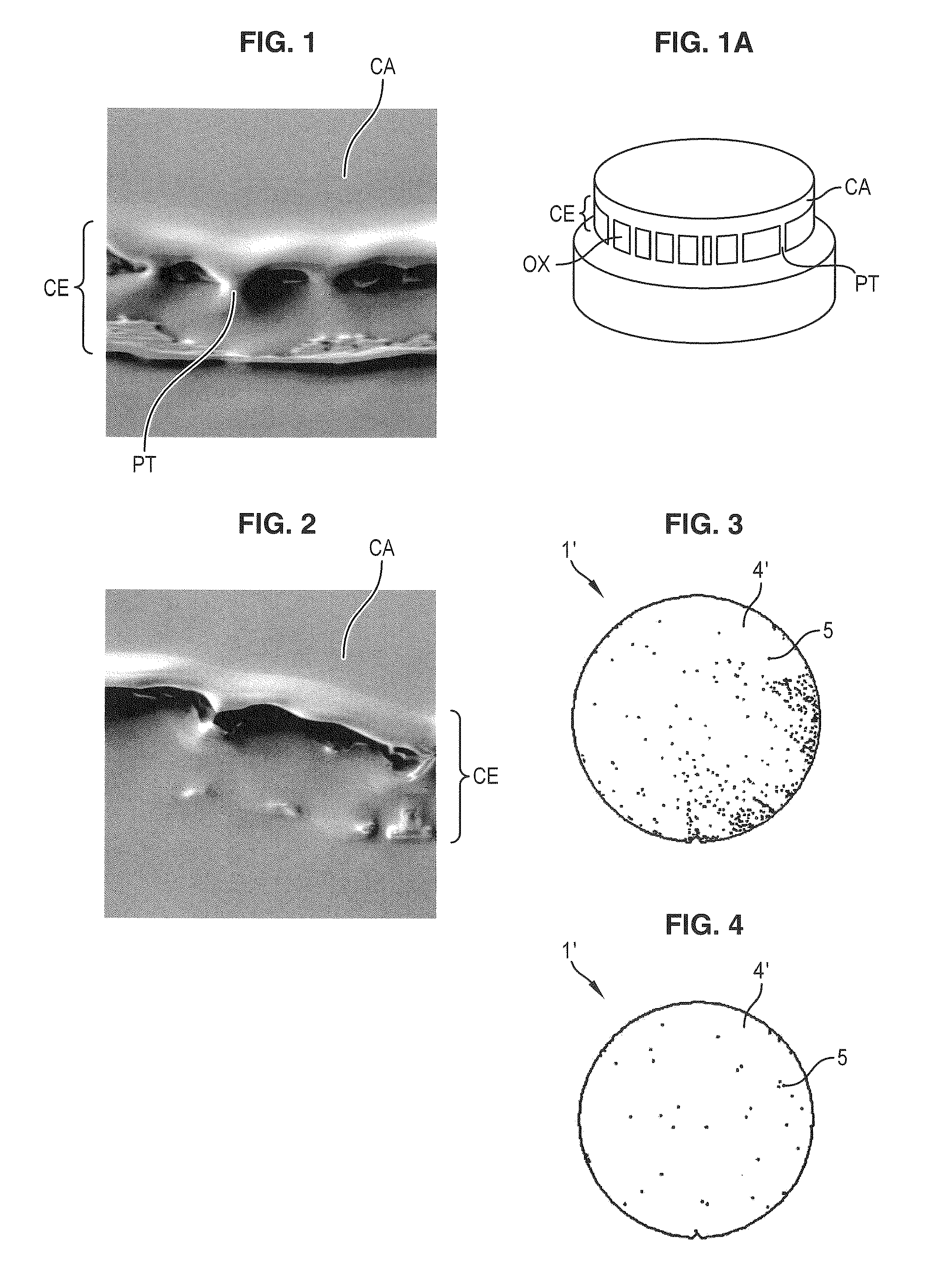
[0043]FIG. 5A illustrates a SOI substrate 1 comprising a carrier substrate 2 in silicon, coated with a layer 3 of silicon oxide SiO2 and a surface layer 4 in silicon.

[0044]The oxide layer 3 is therefore buried between the two layers 2 and 4. Preferably, the thickness of the silicon surface layer is 400 nm or less.

[0045]This SOI substrate may have been obtained, for example, using a layer transfer process using the following chief steps:[0046]creating a weakened region in the thickness of a donor substrate;[0047]forming an oxide layer on the donor substrate (preferably before creating the weakened region), or on a receiver substrate;[0048]bonding the donor substrate and receiver substrate; and[0049]detaching along the weakened region. An example of the transfer process is the SMARTCUT® process of which a description can be found in the work: “Silicon On Insulator Technology:Materials to VLSI, 2nd Edition” by Jean-Pierr...


PUM

PropertyMeasurementUnit
Temperatureaaaaaaaaaa

Abstract

A method to thin an initial silicon-on-insulator substrate that has a layer of silicon oxide buried between a silicon carrier substrate and a silicon surface layer. This method is noteworthy in that it includes conducting a thermal oxidation treatment of the initial substrate to cause oxidation of part of the silicon surface layer and form a thermal oxide thereon; conducting a first cycle of etching followed by cleaning of the silicon surface layer after the thermal oxidation treatment, wherein the etching of the first cycle is conducted so as to fully remove the thermal oxide from the silicon surface layer to thin it and lift off all unstable parts of the initial substrate at edges thereof to form a thinned substrate; conducting, after the first cycle, a second cycle of etching followed by cleaning of the silicon surface layer, wherein the etching of the second cycle is conducted to remove from the surface of the thinned substrate, polluting particles formed during the first etching cycle and that have deposited thereupon, in order to obtain a final SOI substrate having a thinned surface layer that forms an active layer for the substrate.

Description

CROSS-REFERENCE TO RELATED APPLICATION[0001]This application is a 371 filing of International Patent Application PCT / EP2010 / 055198 filed Apr. 20, 2010.BACKGROUND[0002]The invention lies in the area of the fabrication of silicon-on-insulator substrates known to persons skilled in the art under the acronym “SOI.”[0003]A SOI substrate comprises a silicon oxide SiO2 layer, buried between a silicon carrier substrate and a silicon surface layer called the “active layer” since it is on or in this layer that components will subsequently be fabricated intended for applications in the areas of electronics, optics, optoelectronics or microelectronics.[0004]The present invention more specifically concerns a method to thin an initial substrate of SOI type, making it possible to obtain a SOI substrate having a silicon surface layer that is thin, even extra-thin, and whose surface is free or almost free of polluting particles.[0005]The integration of transistors in microelectronics is made with in...

Claims


Application Information

Patent Timeline
IPC IPC(8): H01L21/302H01L21/461C03C15/00C03C25/68H01L21/306H01L21/762
CPCH01L21/30604H01L21/76254
Inventor REYNAUD, PATRICKECARNOT, LUDOVICRADOUANE, KHALID
Owner S O I TEC SILICON ON INSULATOR THECHNOLOGIES
Why Eureka
Try Eureka