Integration of rare-earth doped amplifiers into semiconductor structures and uses of same

a rare earth doped amplifier and semiconductor technology, applied in the direction of semiconductor lasers, optical elements, active medium materials, etc., can solve the problems of real-world fiber loss and dispersion, loss of optical signal strength and/or waveform integrity of optical signals traveling through real-world fibers, and limit the applicable situations in which soa's may be deployed, etc., to achieve low cost and low cost of mass production , the effect of reducing passive waveguide loss

Inactive Publication Date: 2008-10-21
TANG YIN S
View PDF52 Cites 4 Cited by
  • Summary
  • Abstract
  • Description
  • Claims
  • Application Information

AI Technical Summary

Benefits of technology

[0017]In accordance with a further aspect of the present disclosure the REDS layer (Rare-Earth Doped Semiconductor layer) is patterned to further define one or more optical processing elements such as plural waveguides (WG's—or more specifically, Arrayed WaveGuides (AWG's) which can respectively process different wavelengths, thus providing wavelength domain multiplexing and demultiplexing), gratings, phase shift modulators, and optically, electrically and / or mechanically (e.g., MEM's) controlled spatial multiplexers and / or demultiplexers. With the use of semiconductor-based gain media (e.g., monocrystalline silicon that is appropriately doped with one or more rare earth elements) instead of organic-based gain media it becomes possible to provide stable and reliable optical amplification integrally with further optical processing functions such as AWG's, etc. Thus, an integrated, solid-state, planar optical device with good reliability and stability may be provided that can be used with electrical pump energy and / or optical pump energy—where the latter can be a Raman pump or a non-Raman pump. If a Raman pump is used, the device may be structured to reshape (recondition) the optical information contained in the amplified beams, as generally would an O-E-O module that contains electrical amplification means, electrical signal reconditioning and optical signal regeneration means.
[0018]In accordance with further aspects of the present disclosure it will be seen that non-organic materials such as silicon and / or silicon oxide and / or other semiconductors and / or their compounds can be integrally formed as part of a monolithic or other integrated device so as to define an optical gain media that is erbium doped (Er-doped) for use, for example in the 1.5 μm transmission band; and / or that is doped with other rare earth elements such as Nd+ or Yb+ doped for respective use in the 1.34 μm or 1.3 μm bands. Preparation methods for forming the rare earth doped semiconductor regions may include surface plasma deposition of the rare earth elements, and / or inclusion of the rare earth elements in vapor deposition processes (e.g., CVD, ALD, etc.) and / or diffusion, and / or ion implantation of the rare earth elements into the material regions that are to function as optical gain regions. Additionally, concentrations of the incorporated rare earth elements (e.g., Er) in their host materials (e.g., Si or SiO2) may be enhanced by use of respectively more-soluble rare earth compounds (e.g., ErO) that can form solubility-enhancing complexes (e.g., Er—O—Si═Si═ . . . ) with their host materials. Additionally or alternatively, concentrations of the incorporated rare earth elements (e.g., Er) in their host materials (e.g., monocrystalline or polycrystalline Si or SiO2) may be enhanced by trapping them under or between amorphous layers (e.g., amorphous Si and / or amorphous silicon oxide or amorphous silicon nitride) so as to reduce out-diffusion, particularly as a result of rare earth dopant (e.g. Er) activation by rapid thermal annealing or the like.
[0019]In accordance with further aspects of the present disclosure it will be seen that the optical gain regions may be integrated within ridge waveguides, rib waveguides and / or the like and that the latter may define amplifying waveguides, amplifying arrayed waveguides (AWG's), amplifying optical switches and other optical or electro-optical components of suitable small sizes that may be used for photonic integration applications. It will be seen that various optical gain-media pumping methods may be employed including electrical current injection (for generating electrically excited luminescence or electroluminescence); use of 980 nm laser pump and / or use of Raman pumping. It will be seen that various pump energy injection configurations may be used including: non-parallel injection (this including having the pumping beam travel in any direction other than parallel to, and in exactly the same direction as that of the signal beam) and more specifically, having the pumping beam travel generally perpendicularly to the information-carrying, signal beam and repeatedly bouncing the pumping beam back and forth in non-parallel fashion within the gain media so as to increase the number of signal-amplifying interactions occurring between the triad of the pumping beam, the signal beam, and the available concentration of rare earth atoms. More specifically, metallic or other mirrors may be used to provide multiple internal reflection of the pump energy through the gain media to thereby increase pumping efficiency and reduce pump-to-signal interference and to thereby produce an easily-extractable output signal beam that has improved signal to noise ratio).
[0021]It will be seen that the integrally formed, optical-gain regions may be used to monolithically form Erbium Doped Planar Amplifiers (EDPA's) or Erbium Doped Planar Raman Amplifier (EDPRA's) for use with on-the-fly optical signal regeneration (that is, without the need for O-E-O conversion), as well as for use in eliminating passive waveguide loss in integrated photonic components and modules. Devices built in accordance with the disclosure may be made compact in size, cheap to mass produce and with the reliability and consistency advantages associated with electronic integrated circuits made of similar semiconductor materials (e.g., Si that is doped only with electrical conductivity providing dopants, SiO2 and the like). It will be seen that devices built in accordance with the disclosure may be made suitable for on-chip integration of photonic, electronic, and / or electro-photonic functionalities so as to increase overall usefulness without substantial sacrifice of device performance.
[0022]A method in accordance with the present disclosure for mass producing integrated photonic and / or electro-photonic devices may include the steps of: (a) incorporating one or more rare earth elements with appropriate concentrations into silicon and / or silicon oxide and / or into other semiconductors and / or their dielectric compounds, where the incorporation may occur as the semiconductor and / or semiconductor compound regions are being grown or otherwise formed directly on a monolithically integrated device or as they are formed for subsequent bonding to the monolithically integrated device and where the incorporation correspondingly defines one or more optical gain media regions within the integrated device; (b) defining respective signal input ports in the integrated device for receiving input optical signals into corresponding ones of the one or more optical gain media regions; (c) defining respective pump energy receiving means in the integrated device for receiving pump energy into corresponding ones of the one or more optical gain media regions; and (d) defining respective signal output means in the integrated device for outputting optical signals from corresponding ones of the one or more optical gain media regions. The fabrication process may further include the formation of appropriate pump energy guiding means for guiding radiative pump energy and / or injected electrical current into the one or more optical gain media regions for promoting interaction between the pump energy, the input optical signal(s) and the incorporated, rare earth elements. The incorporation of the one or more rare earth elements may include the provision of one or more binding agents such as oxygen for enhancing binding between the rare earth elements (e.g., Er) and the host material (e.g., monocrystalline Si) and / or the provision of one or more trapping layers (e.g., amorphous Si and / or amorphous silicon oxide) so as to reduce out-diffusion of the incorporated rare earth element(s) and / or the provision of one or more rapid thermal treatment steps so as to activate the incorporated rare earth element(s) within their respective parts of the host material.

Problems solved by technology

However, real-world fibers exhibit loss and dispersion.
As a result, optical signals traveling through real-world fibers lose optical signal strength and / or waveform integrity.
This fundamentally limits the applicable situations in which SOA's may be deployed.
Although the performance of the newer Raman amplifiers (EDRA's) is very good, the cost of a discrete EDRA amplifier module tends to be very high; much higher than the already costly, discrete EDFA modules.
Additionally, both of conventional EDRA's and EDFA's suffer the drawbacks of having very large physical sizes and high power consumptions.
These proposals have drawbacks.
Polymer based materials tend to be unstable and unreliable due to their organic material nature (e.g., they tend to have large and disorderly molecule chains with embedded holes that can trap gases and / or release or absorb gases from the environment, this making the polymer-based amplifiers very sensitive to environmental changes such as changes in temperature and / or humidity).
Because of these drawbacks, the industry still lacks a practical way for providing integrated optical signal amplification without incurring the high cost, large module size, and the high power consumption typically associated with discrete versions of EDRA's and EDFA's.

Method used


Image

  • Integration of rare-earth doped amplifiers into semiconductor structures and uses of same
  • Integration of rare-earth doped amplifiers into semiconductor structures and uses of same
  • Integration of rare-earth doped amplifiers into semiconductor structures and uses of same

Examples


Embodiment Construction

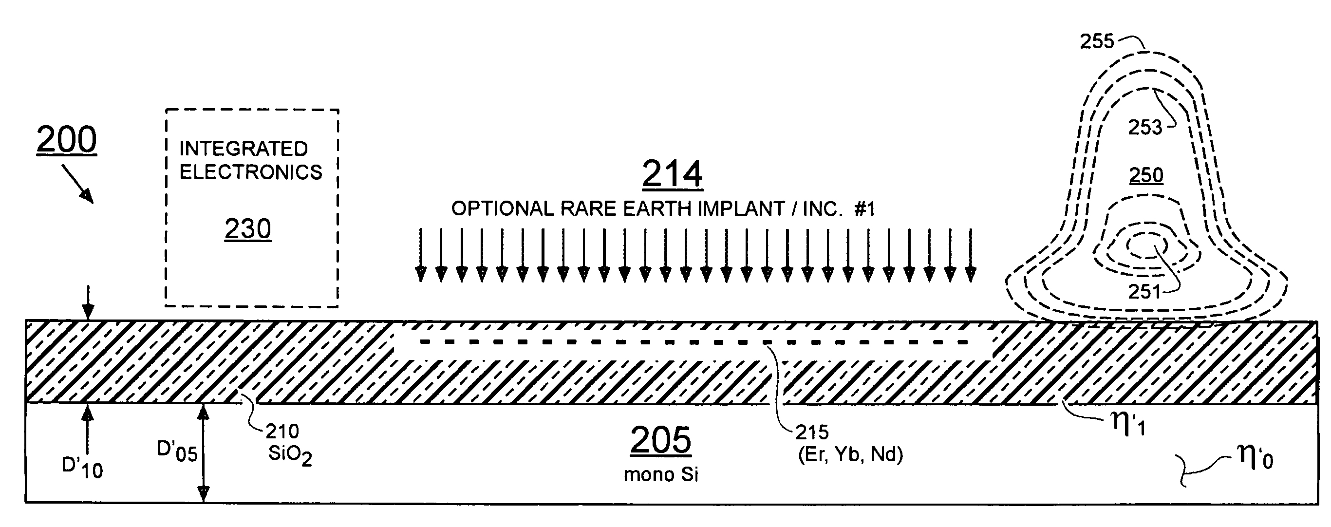
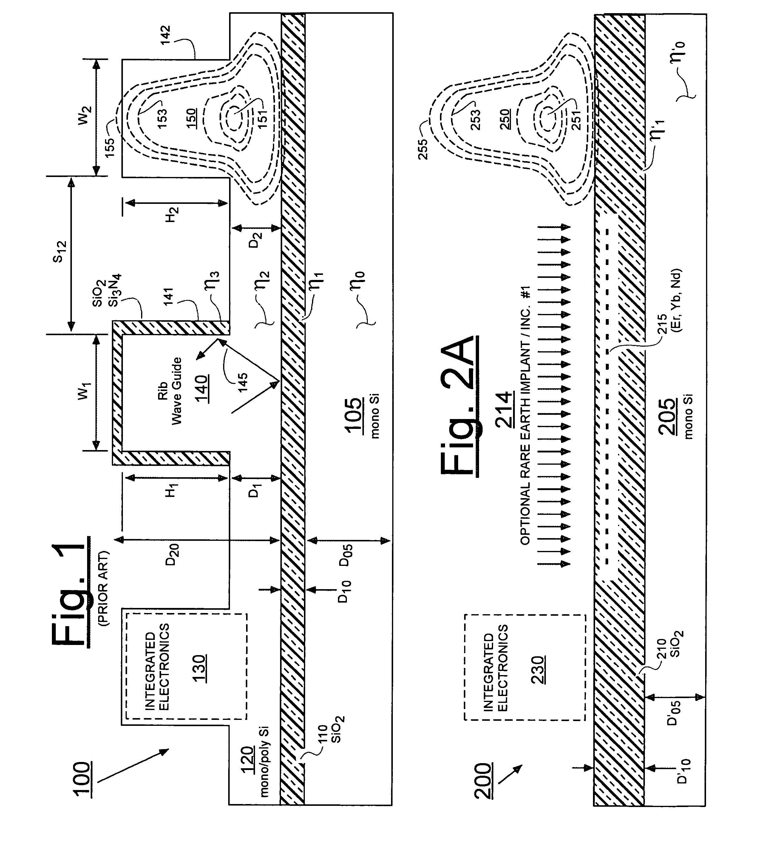
[0032]FIG. 1 is a combination of introductory block diagram and a cross-sectional side view of a conventional SOI (silicon on insulator) integrated device 100 whose upper silicon layer has been patterned to define a pair of rib-style optical waveguides. The rib portions are identified as 140 and 142. An integrated electronics circuit is schematically shown to be present in or around region 130.

[0033]More specifically, the illustrated device 100 is structured to have a monocrystalline silicon substrate 105 having a respective first refractive index, n0, and a respective first thickness, D05. A silicon dioxide layer 110 has been thermally grown or has been otherwise formed on the substrate 105 to provide a second layer of a respective second refractive index, n1, and a respective second thickness, D10. A polysilicon layer 120 (it could be or include amorphous material) has been provided on top of layer 110 by, for example, chemical vapor deposition (CVD) or otherwise to thereby provid...


PUM


Abstract

An integrated device is disclosed which has a substrate and a Rare-Earth Doped Semiconductor layer (REDS layer) integrated with the substrate. The REDS layer is patterned to define one or more optically amplifying structures each having a first I / O port for receiving or outputting a first optical signal, and at least one pump energy receiving port for receiving pumping energy in the form of at least one of electrical pump energy and / or optical pump energy. In one particular set of embodiments, at least one of the optical amplifying structures is a Raman type amplifier where a corresponding pump energy receiving port is structured for receiving Raman type pumping energy having an effective frequency which is about one optical phonon frequency higher than a signal frequency of an optical signal supplied at a corresponding I / O port. Methods are disclosed for fabricating Rare-Earth Doped Semiconductor layers, including providing such layers in semiconductor-on-insulator (SOI) structures and for enhancing the effective, long-term concentrations of incorporated, rare earth atoms. Additionally, non-parallel pumping techniques are disclosed.

Description

FIELD OF DISCLOSURE[0001]The present disclosure of invention relates generally to solid state amplification of optical signals in photonic structures such as in monolithically integrated structures.[0002]The disclosure relates more specifically to the provision of rare-earth doped gain regions into photonic and / or electro-optical structures and to uses of the same.CROSS REFERENCE TO PATENTS[0003]The disclosures of the following U.S. patents are incorporated herein by reference:[0004](A) U.S. Pat. No. 6,292,288, Akasaka et al, Sep. 18, 2001 {Short abstract: Semiconductor lasers are multiplexed together to pump Er-doped fiber for flattened power output};[0005](B) . . . In order to avoid front end clutter, this cross referencing section (2) continues as (2′) at the end of the disclosure, slightly prior to recitation of the patent claims. Additional, non-patent material is also cited there.DESCRIPTION OF RELATED ART[0006]Discrete optical fibers are typically used as the primary building...

Claims


Application Information

Patent Timeline
Patent Type & Authority Patents(United States)
IPC IPC(8): H01S5/00H04B10/12H01S3/00H01S3/063H01S3/09H01S3/16
CPCH01S3/0632G02B2006/12097H01S3/0637H01S3/2308H01S3/1608H01S3/1691H01S3/09
Inventor TANG, YIN S.
Owner TANG YIN S
Why Eureka
Try Eureka