

Method for implantation of high dopant concentrations in wide band gap materials
a wide band gap material and high concentration technology, applied in the direction of basic electric elements, semiconductor/solid-state device manufacturing, electrical equipment, etc., can solve the problems of inability to lateral dopant film growth in microcircuits, difficult to incorporate dopants by diffusion into many of these materials, and high concentration of wide band gap materials, so as to minimize the defect concentration and reduce the concentration of defects , the effect of rapid thermal annealing
- Summary
- Abstract
- Description
- Claims
- Application Information
AI Technical Summary
Benefits of technology
Problems solved by technology
Method used
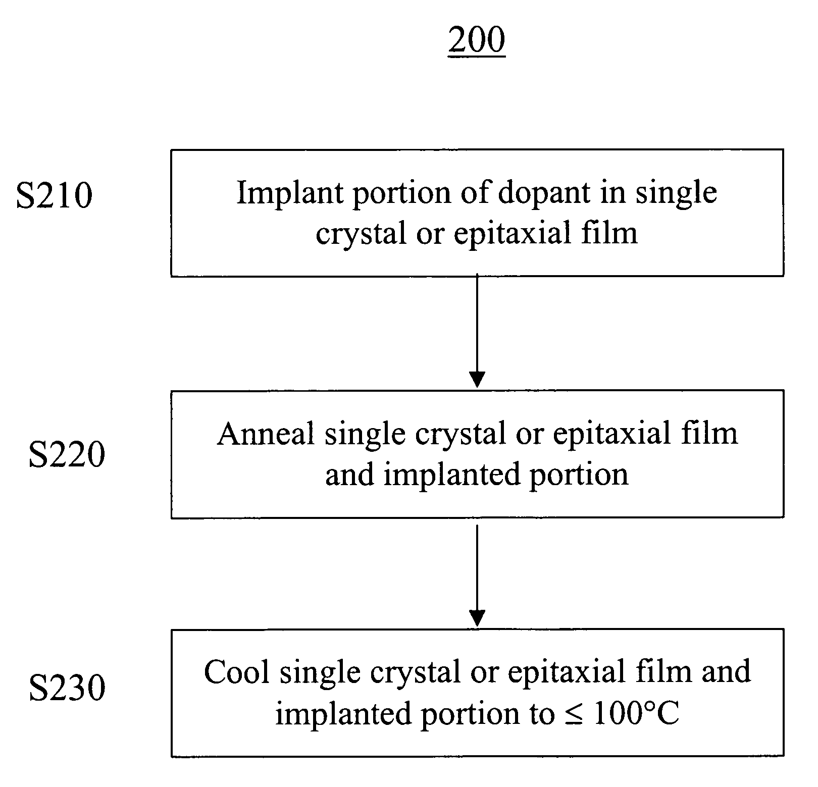
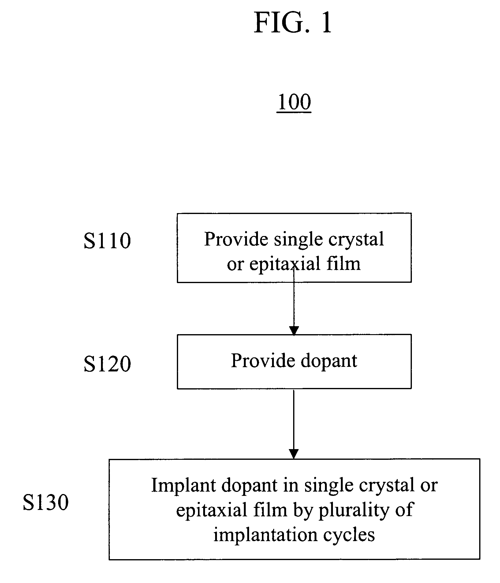
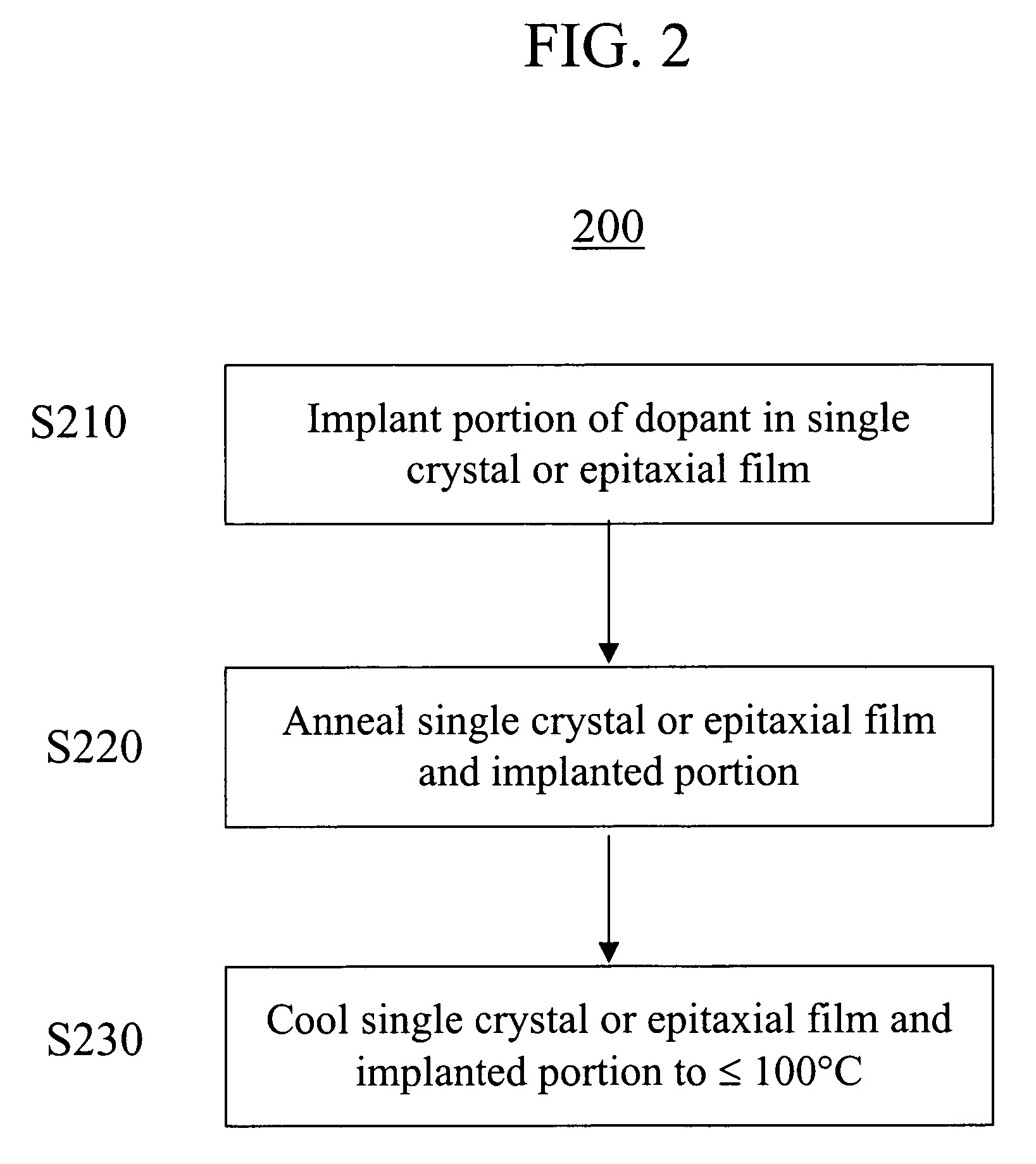
Image

Examples
example 1
[0035]The effectiveness of LMDI RTA technique described herein was investigated for lattice recovery of GaN implanted with Mg+ ions. Two 1 μm GaN single crystal films were implanted at room temperature with 50 keV Mg+ ions. Sample 1 was implanted in a single step to obtain a dose of 6×1015cm−2 of Mg+ ions and then annealed three times at 900° C. for 30 seconds. Sample 2 was implanted in three steps to obtain the same total ion dose (6×1015cm−2). The ion dose for each step was 2×1015cm−2. Each implantation step was followed by a single annealing step at 900° C. for 30 sec. Thus, both Sample 1 and Sample 2 were implanted to the same total Mg+ ion dose (6×1015cm−2) and annealed three times under the same conditions.
[0036]The amount of lattice damage to each sample was measured by Rutherford backscattering spectroscopy combined with channeling (RBS / C) and is shown in FIG. 5. In FIG. 5: (a) is a random unaligned RBS spectrum; (b) is a spectrum of a 1 μm GaN single crystal film implanted ...
PUM
 Abstract
Description
Claims
Application Information