Light emitting diode crystalline grain

A technology for light-emitting diodes and crystal grains, which is applied to electrical components, circuits, semiconductor devices, etc., can solve the problems of affecting the light-emitting efficiency of light-emitting diode crystal grains and unfavorable epitaxial layer structure.

Inactive Publication Date: 2013-04-24
ZHANJING TECH SHENZHEN +1
View PDF4 Cites 6 Cited by
  • Summary
  • Abstract
  • Description
  • Claims
  • Application Information

AI Technical Summary

Problems solved by technology

[0003] However, the epitaxial layer structure grown sequentially on the substrate usually has a vertical sharp corner away from the top edge of the substrate, see figure 1 , some light emitted from the active layer 3, such as light A with an angle γ between the active layer 3

Method used


Image

  • Light emitting diode crystalline grain
  • Light emitting diode crystalline grain
  • Light emitting diode crystalline grain

Examples


Embodiment Construction

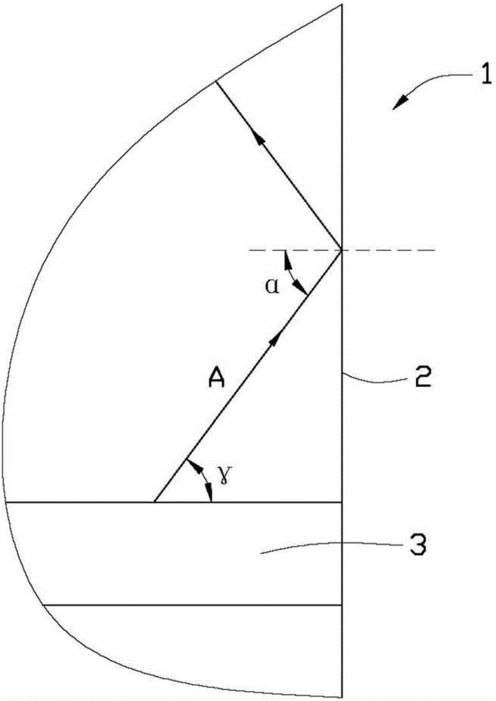
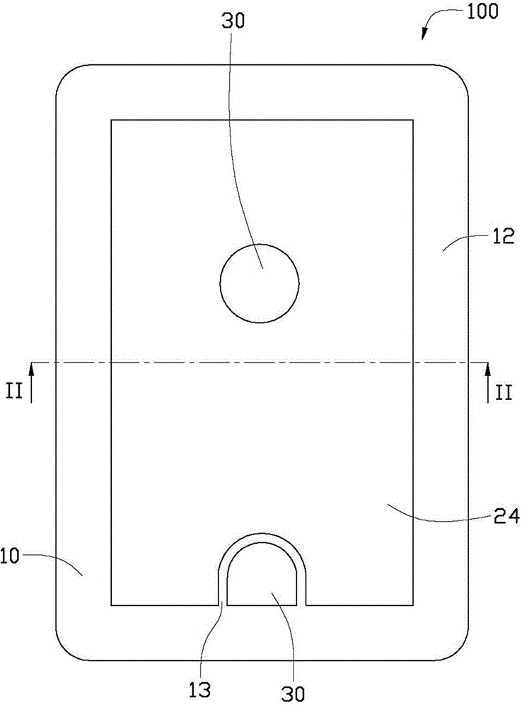
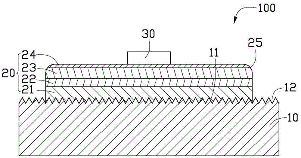
[0014] see figure 2 and image 3 The light emitting diode die 100 provided in the embodiment of the present invention includes a substrate 10 , an epitaxial layer 20 grown on the substrate 10 , and an electrode 30 .

[0015] The substrate 10 is a patterned substrate, which includes an upper surface 11 formed with microstructures. The material of the substrate 10 can be sapphire (Al 2 o 3 ), silicon carbide (SiC), silicon (Si), gallium nitride (GaN) or zinc oxide (ZnO), depending on the desired physical and optical properties and cost budget. The shape of the substrate 10 is not limited, and may be a rectangle, a circle, etc. In this embodiment, the substrate 10 is a rectangle with four sides.

[0016] The epitaxial layer 20 is formed on the upper surface 11 of the substrate 10 , and the epitaxial layer 20 covers part of the substrate 10 . Specifically, the upper surface 11 of the substrate 10 is exposed to the air and surrounds the epitaxial layer 20 to form a cutting li...


PUM


Abstract

A light emitting diode crystalline grain comprises a substrate and an epitaxial layer which is formed on the substrate. The substrate comprises an upper surface. The epitaxial layer comprises a first semiconductor layer close to the substrate, a second semiconductor layer far away from the substrate, and an active layer arranged between the first semiconductor layer and the second semiconductor layer. The edge of the top, far away from the substrate, of the epitaxial layer is provided with an arc angle or a slant chamfer, and therefore light can be emitted from the side face of the epitaxial layer favorably, and luminous efficiency of the light emitting diode crystalline grain is improved.

Description

technical field [0001] The invention relates to a semiconductor structure, in particular to a light emitting diode crystal grain. Background technique [0002] Existing light emitting diode (Light Emitting Diode, LED) grains include a substrate, an epitaxial layer structure grown on the substrate, and electrodes. The epitaxial layer structure usually includes an N-type semiconductor layer, an active layer, and a P-type semiconductor layer, which are sequentially grown upward from the substrate. In order to make the current evenly distributed and improve the luminous efficiency of the grain, the industry usually adds a transparent electrode between the P-type semiconductor layer and the electrode. [0003] However, the epitaxial layer structure grown sequentially on the substrate usually has a vertical sharp corner away from the top edge of the substrate, see figure 1 , some light emitted from the active layer 3, such as light A with an angle γ between the active layer 3 an...

Claims


Application Information

Patent Timeline
IPC IPC(8): H01L33/20
CPCH01L33/22H01L33/20H01L33/42
Inventor 洪梓健沈佳辉彭建忠
Owner ZHANJING TECH SHENZHEN
Why Eureka
Try Eureka