Plasma laser device

A plasma and laser technology, which is applied to the structure of optical waveguide semiconductors, can solve problems such as unfavorable miniaturization of devices, unfavorable laser devices, and large volume, and achieve the effects of being conducive to miniaturization, strong binding ability, and size reduction

Active Publication Date: 2013-04-24
张昭宇
View PDF2 Cites 9 Cited by
  • Summary
  • Abstract
  • Description
  • Claims
  • Application Information

AI Technical Summary

Problems solved by technology

[0005] However, the above-mentioned surface plasmon laser is based on a linear nanowire structure with a length of 1-2 microns and a large volume. If it is used in an integrated optical system, it is not conducive to the miniaturization of the device; at the same time, the laser in the above structure relies on Laser light is generated by the reflection of the two ends of the nanowire, most of the energy is emitted from the end face, and the energy left in the laser is very little, which is not conducive to obtaining high-power laser devices

Method used


Image

  • Plasma laser device
  • Plasma laser device
  • Plasma laser device

Examples


Embodiment 1

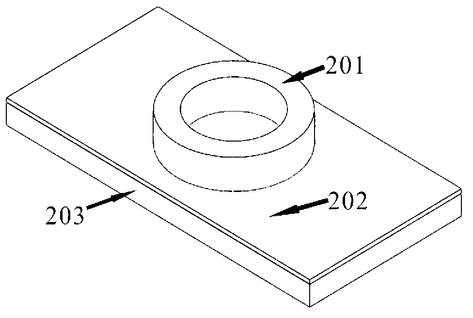
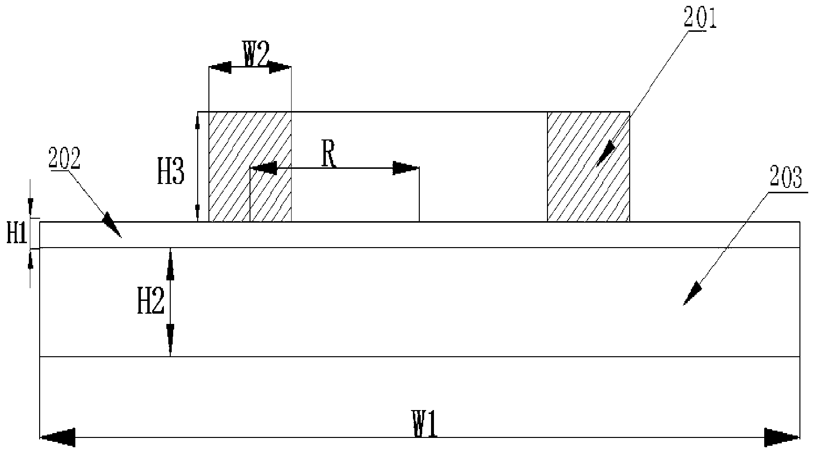
[0039] Please refer to figure 2 , a plasma laser provided in an embodiment of the present application, including a metal layer 203, a low-refractive-index medium layer 202 formed on the metal layer 203, and a ring-shaped gain medium layer formed on the low-refractive-index medium layer 202 201 , the cross section of the gain medium layer 201 closest to the metal layer 203 falls within the range covered by the metal layer 203 . In other embodiments, the low-refractive-index medium layer 202 may not be included, but only the double-layer structure of the metal layer 203 and the annular gain medium layer 201 .

[0040] The cross-sectional shape of the gain medium layer 201 is a rectangle, and may be any one of an oval ring, a hexagonal ring, a square ring, a trapezoidal ring, and a triangular ring. The ring-shaped gain medium layer 201 formed in this example reduces the contact surface with the low-refractive index medium layer, thereby reducing metal loss. At this time, light...

Embodiment 2

[0052] Such as Figure 7 As shown, another structural plasmonic laser of the present application includes a gain medium layer 301 and a metal layer 302, wherein the cross section of the gain medium layer 301 parallel to the metal layer 302 is an elliptical ring structure.

[0053] Due to the effect of surface plasmons, the optical field is limited to the contact surface of the metal layer 301 and the gain medium layer 302. At the same time, since the contact surface of the metal layer 301 and the gain medium layer 302 is annular, that is, the contact surface is very small, thereby reducing the The loss to the metal is reduced, and the light circulates along the annular contact surface, which can also produce a good coupling effect.

[0054] In another embodiment, a low-refractive index medium layer may also be formed between the gain medium layer 301 and the metal layer 302, and the cross section of the gain medium layer 301 closest to the metal layer 302 falls within the rang...


PUM


Abstract

The invention discloses a plasma laser device which comprises a metal layer and a gain medium layer formed on the metal layer. The transversal section of the gain medium layer is ring-shaped, wherein the transversal section of the gain medium layer is parallel to the metal layer. The transversal section of the gain medium layer closest to the metal layer is dropped in the scope covered by the metal layer. As the plasma laser device is provided with the ring-shaped gain medium layer, light field can do syntony in the ring-shaped structure so that the light field is strong in constraint ability. The light field can transmit circularly on the surface, wherein the surface is formed between the gain medium layer and the metal layer. The size of a nanometer laser device can be decreased. Meanwhile, integrated optics system can be miniaturized favorably as the ring-shaped structure can produce couple effects easily.

Description

technical field [0001] This application relates to the field of micro-nano optoelectronic devices / lasers, in particular to a plasma laser. Background technique [0002] Nanophotonics and optoelectronics have developed rapidly in recent years. Due to their excellent optical and electrical properties, nanostructured devices have been widely used in various optical and optoelectronic devices, covering a range from waveguides to laser radiation. With the rise of nanotechnology, the study of nanolasers has become a new and important topic. Nanolasers have strong application value in many fields, including electronic communication, information storage, biochemical sensors, and nanolithography. [0003] At present, many researchers apply the concept of surface plasmons to the laser field, and use the feature of surface plasmons to break through the diffraction limit, and are committed to the miniaturization of laser components. [0004] figure 1 It is a nano-laser based on the ...

Claims


Application Information

Patent Timeline
Patent Type & Authority Applications(China)
IPC IPC(8): H01S5/20
Inventor 刘旭东张昭宇郭思尧苏光耀肖登
Owner 张昭宇
Why Eureka
Try Eureka