Broadband surface plasma logic input source

A surface plasmon and logic input technology, applied to the structure/shape of optical resonators, can solve the problems of miniaturization of scale and limitation of integration degree, and achieve the effect of miniaturization, strong binding ability and size reduction

Active Publication Date: 2016-05-18
UNIV OF SHANGHAI FOR SCI & TECH
View PDF5 Cites 7 Cited by
  • Summary
  • Abstract
  • Description
  • Claims
  • Application Information

AI Technical Summary

Problems solved by technology

Traditional optical devices are constrained by the diffraction limit, and their miniaturization and integration are limited. However, the characteristics of surface plasmons can break through the diffraction limit well, and are used in high-speed optical communications for the manufacture of integrated optical circuits based on surface plasmons. provides the possibility

Method used


Image

  • Broadband surface plasma logic input source
  • Broadband surface plasma logic input source
  • Broadband surface plasma logic input source

Examples


Embodiment 1

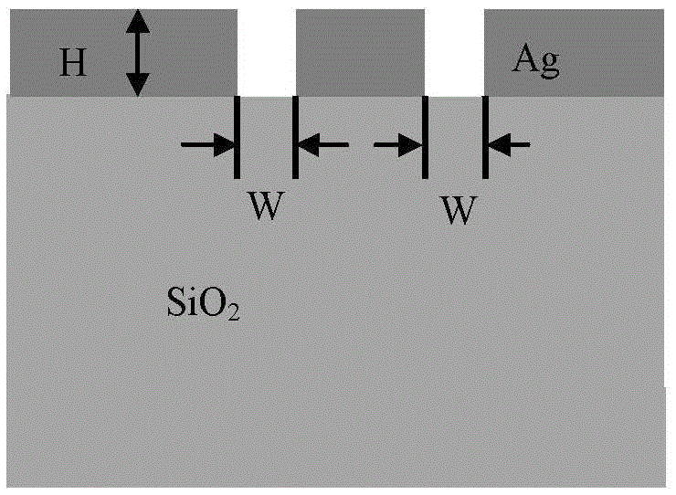
[0024] Please refer to figure 1 , figure 1 A structural diagram of a broadband surface plasmon logic input source provided in an embodiment of the present application includes a base layer-a metal layer, the base material is silicon dioxide, and the metal layer material is silver.

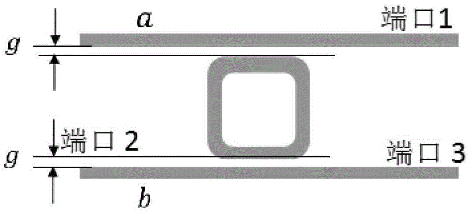
[0025] Please refer to image 3 , image 3 A top view structure diagram of a broadband surface plasmon logic input source provided in an embodiment of the present application, including two rounded rectangular rings etched with a focused ion beam and waveguides on both sides of the rectangular ring, in which two rounded rectangular rings The rings are arranged horizontally.

[0026] In this example, the thickness of the metal layer is 60 nm, the width of the waveguides on both sides of the rectangular ring is 80 nm, and the width of the rectangular ring is 80 nm.

[0027] The structure of broadband surface plasmons in this example is simulated by using COMSOL.

[0028] Figure 5 It is a distr...

Embodiment 2

[0031] Please refer to figure 1 , figure 1 A cross-sectional structure diagram of a broadband surface plasmon logic input source provided in an embodiment of the present application includes a base layer-a metal layer, the base material is silicon dioxide, and the metal layer material is silver.

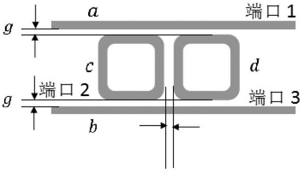
[0032] Please refer to Figure 4 , Figure 4 A top view structure diagram of a broadband surface plasmon logic input source provided in an embodiment of the present application, including two rounded rectangular rings etched with a focused ion beam and waveguides on both sides of the rectangular ring, in which two rounded rectangular rings The rings are arranged vertically.

[0033] In the broadband surface plasmon logic input source of this application, due to the use of the ring waveguide structure, the resonant light field in the ring structure has a strong confinement ability, and because the light field propagates circularly on the surface of the rectangular ring area, it red...


PUM


Abstract

The invention relates to a broadband surface plasma logic input source which comprises a substrate layer and a metal layer. The substrate layer is made of a low-refractive-index material. The metal layer is formed above the substrate layer. A plurality of rectangular rings with four smooth corners and waveguides at two sides of the rectangular rings are etched on the metal layer through focused ion beam etching, wherein the rectangular rings with four corners can be arranged parallelly or vertically. The rectangular rings which are etched on the metal layer and four smooth corners and the waveguides at two sides of the rectangular ring form the broadband surface plasma logic input source. According to the broadband surface plasma logic input source, An optical field resonates at an interface between an air medium and the metal. Because the metal layer is provided with the rectangular ring structures with four smooth corners each and waveguides at two sides of the rectangular ring, resonance between a resonance electromagnetic wave and the annular structure occurs. An annular resonance chamber realizes relatively high inhibition for the optical field. Because the optical field with a specific wavelength is inhibited on the metal surface layer and is propagated circularly, the dimension of the device can be effectively reduced. Furthermore on condition of broadband, partial light is emitted out of ports along the waveguides at two sides of the rectangular rings, thereby realizing a logic gate.

Description

technical field [0001] The invention belongs to the field of optoelectronic devices, in particular to an optical resonator and a logic AND gate. Background technique [0002] Because resonator structures can be applied to high-performance quantum optical devices, optical sensors and low-energy-loss optoelectronic devices, research on resonator structures has developed rapidly in recent years, and various resonator structures have sprung up, such as Photonic crystal resonators and dielectric disk resonators, etc. Although these resonators exhibit good performance, they cannot break through the diffraction limit size limit and cannot realize the miniaturization of devices. [0003] Existing research attempts to apply surface plasmon polariton (SurfacePlasmonPolariton, SPP) to the resonator structure. Surface plasmon is an electromagnetic wave mode caused by the interaction between light and free electrons on the metal surface. It is confined near the metal-medium interface a...

Claims


Application Information

Patent Timeline
Patent Type & Authority Applications(China)
IPC IPC(8): H01S3/08
CPCH01S3/08
Inventor 文静朱梦均钟阳万王康冯辉张大伟
Owner UNIV OF SHANGHAI FOR SCI & TECH
Why Eureka
Try Eureka