P-type disposable programmable device structure

A device structure, one-time technology, applied in the semiconductor field, can solve the problems of low read current, large OTP peripheral circuit area, consumption, etc.

Active Publication Date: 2013-05-08
SHANGHAI HUAHONG GRACE SEMICON MFG CORP
View PDF4 Cites 5 Cited by
  • Summary
  • Abstract
  • Description
  • Claims
  • Application Information

AI Technical Summary

Problems solved by technology

However, if the substrate voltage is too high, the read current will be too low, and the read circuit cannot distinguish the current of the OTP cell after programming; if the substrate voltage is too low, the initial current of the OTP cell before programming is too large, and it cannot be read. Differentiate the state of the OTP unit
Therefore, it usually requires a very complicated peripheral reading circuit to provide two accurate voltages to the substrate and the source at the same time, which will consume a large amount of OTP peripheral circuit area.
Although the unit area of ​​each P-type OTP device is very small, more peripheral circuits limit the application of this type of device to applications that require high-density capacity

Method used


Image

  • P-type disposable programmable device structure
  • P-type disposable programmable device structure
  • P-type disposable programmable device structure

Examples


Embodiment Construction

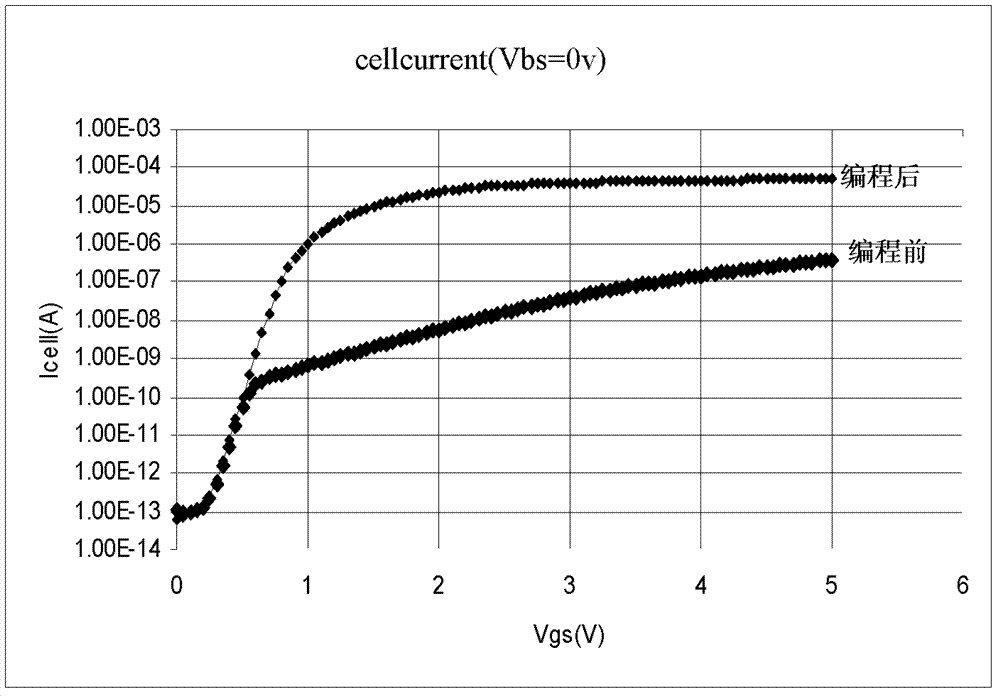
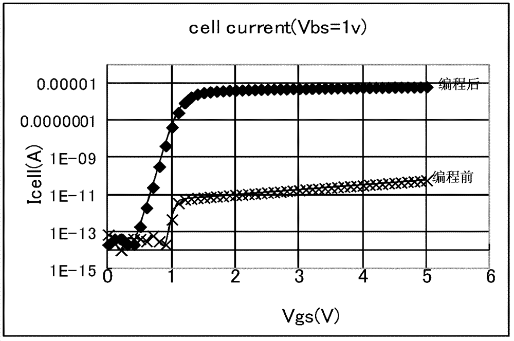
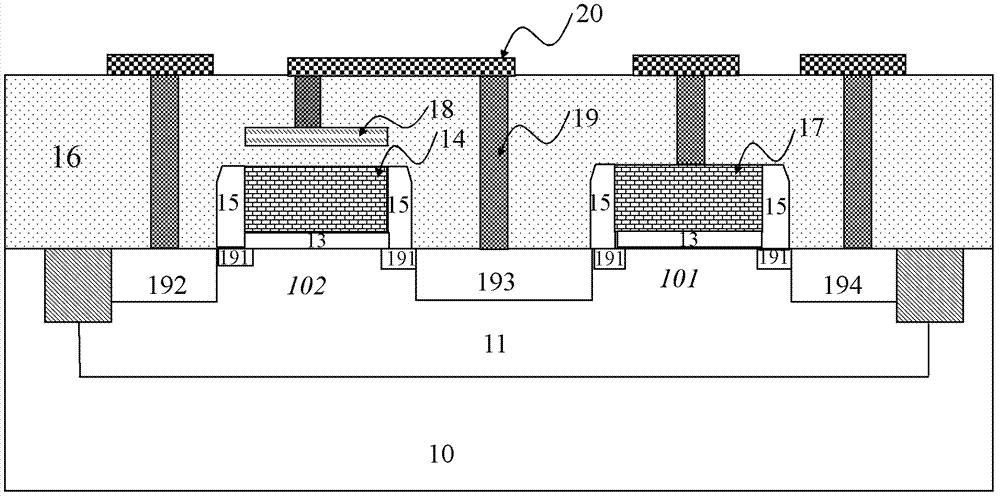
[0021] The first embodiment of the P-type one-time programmable device structure of the present invention is as follows image 3 As shown, an N-type well 11 is formed on the silicon wafer 10, and a first P-type heavily doped region 192, a second P-type heavily doped region 193, and a first P-type heavily doped region 193 are sequentially formed on the N-type well 11 from left to right. Three P-type heavily doped regions 194, on the N-type well 11 between the first P-type heavily doped region 192 and the second P-type heavily doped region 193 and between the second P-type heavily doped region 193 and the third P-type Gate oxides 13 are respectively formed on the N-type wells 11 between the first P-type heavily doped regions 194 and the gate oxides 13 between the first P-type heavily doped regions 192 and the second P-type heavily doped regions 193. Storage tube gate polysilicon 14, gate oxide 17 is formed on the gate oxide 13 between the second P-type heavily doped region 193 a...


PUM


Abstract

The invention discloses a P-type disposable programmable device structure. An N-type trap is formed on a silicon wafer; a first P-type heavily doped region, a second P-type heavily doped region and a third P-type heavily doped region are sequentially formed on the N-type trap from left to right; gate-oxide is formed on the N-type trap between the first P-type heavily doped region and the second P-type heavily doped region and on the N-type trap between the second P-type heavily doped region and the third P-type heavily doped region; storage tube grid polycrystalline silicon is formed on the gate-oxide between the first P-type heavily doped region and the second P-type heavily doped region; gate tube grid polycrystalline silicon is formed on the gate-oxide between the second P-type heavily doped region and the third P-type heavily doped region; an electricity conductive layer is formed above the storage tube grid polycrystalline silicon; and a dielectric layer is formed between the electricity conductive layer and the storage tube grid polycrystalline silicon. The P-type disposable programmable device structure improves conductive currents of the whole device after programming, and increases current ranges capable of being distinguished before and after the programming.

Description

technical field [0001] The invention relates to semiconductor technology, in particular to a P-type one-time programmable (One Time Program, OTP) device structure. Background technique [0002] The existing P-type OTP device is a one-time programmable device formed by connecting two PMOS transistors in series. The first PMOS transistor is used as a gate transistor, and the source of the first PMOS transistor is formed by using a P-type diffusion region in an N-type well. Pole and drain, the gate of the first PMOS transistor is used as the word line of the entire device, the source of the first PMOS transistor is used as the source of the entire device; the second PMOS transistor is used as the storage unit of the OTP device , the gate of the second PMOS transistor is floating, and the source and drain of the second PMOS transistor are formed in the N-type well with a P-type diffusion region, and the drain of the second PMOS transistor is used as the whole The bit line of th...

Claims


Application Information

Patent Timeline
Patent Type & Authority Applications(China)
IPC IPC(8): H01L27/112G11C17/08
Inventor 刘梅黄景丰
Owner SHANGHAI HUAHONG GRACE SEMICON MFG CORP
Why Eureka
Try Eureka