Semiconductor device

A semiconductor and device technology, applied in the field of semiconductor devices to achieve high reliability

Inactive Publication Date: 2013-05-15
HITACHI LTD
View PDF10 Cites 2 Cited by
  • Summary
  • Abstract
  • Description
  • Claims
  • Application Information

AI Technical Summary

Problems solved by technology

In addition, in Non-Patent Document 3, it is described that a chalcogenide material requires about 120 ns for low resistance and about 50 ns for high resistance.

Method used


Image

  • Semiconductor device
  • Semiconductor device
  • Semiconductor device

Examples


Embodiment approach

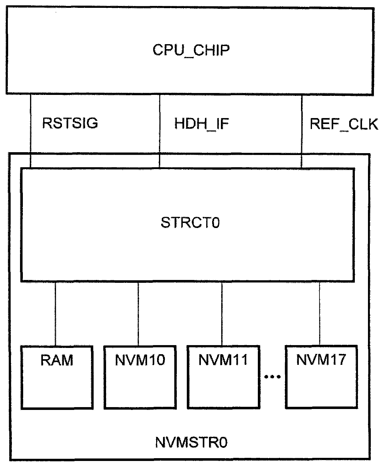
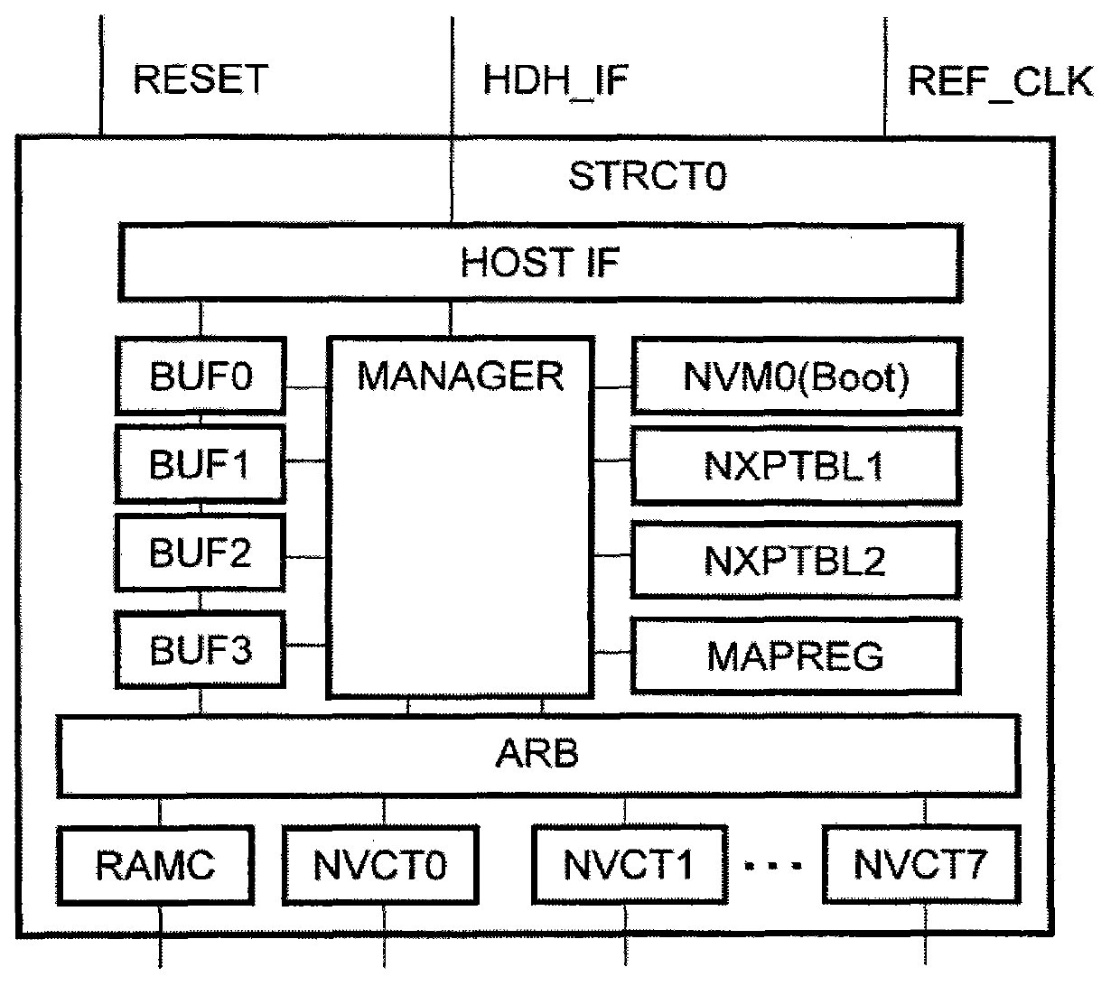
[0133] use Figure 2 to Figure 35 An information processing system to which an embodiment of the present invention is applied will be described.

[0134] figure 2 It is a block diagram showing an example of the configuration of an information processing system device composed of an information processing device CPU_CHIP and a memory module NVMSTR0 according to an embodiment of the present invention. Such as figure 2 As shown, the information processing device CPU_CHIP is not particularly limited, but here is a host controller that manages data stored in the memory module NVMSTR0 with a logical address LAD in units of at least 512 bytes. Data is read or written to the memory block NVMSTR0 through the interface signal HDH_IF.

[0135] The signal system for connecting the information processing device CPU_CHIP and the memory module NVMSTR0 includes a serial interface signal system, a parallel interface signal system, an optical interface signal system, and the like. It goes...


PUM


Abstract

An object of the present invention is to realize a highly reliable long-life information processor capable of high-speed operation and easy to handle. The processor includes a semiconductor device comprising a nonvolatile memory device including a plurality of overwritable memory cells, and a control circuit device for controlling access to the nonvolatile memory device. The control circuit device sets assignments of second addresses to the nonvolatile memory device independently of first addresses externally supplied, such that the physical disposition of part of the memory cells used for writing of first data to be written externally supplied is one of the first to (N+1)th of every (N+1) memory cells (N: a natural number) at least in one direction. Accordingly, an information processing device having the advantages of high reliability, long service lifetime, high work speed, and convenient use is realized.

Description

technical field [0001] The present invention relates to semiconductor device technology including nonvolatile memory devices. Background technique [0002] In recent years, SSDs (Solid State Drives) including a plurality of NAND-type flash memories and controllers have been used in server devices, laptop personal computers, notebook computers, and the like. For example, Non-Patent Document 4 discloses that there is an upper limit to the number of times of erasing in a NAND flash memory, and that there is a large difference between the data writing size and the data erasing size. In addition, for example, Patent Document 1, Patent Document 2, Patent Document 3, and Patent Document 4 disclose a method of controlling a NAND flash memory. [0003] Also, among the techniques studied by the inventors of the present invention, there is, for example, a semiconductor device including a phase-change memory. Such memories use chalcogenide materials (or phase change materials) such as...

Claims


Application Information

Patent Timeline
Patent Type & Authority Applications(China)
IPC IPC(8): G06F12/06G06F3/06
CPCG06F12/02G06F12/0246G06F11/1072G11C14/009G11C29/52
Inventor 三浦誓士
Owner HITACHI LTD
Why Eureka
Try Eureka