Chip observation sample manufacture method and system

A sample production and chip technology, which is applied in the field of chip observation sample production method and system, can solve the problems of not having universal applicability, large floor area, high price, etc., and achieve the goal of improving universal applicability, making conveniently, and improving efficiency Effect

Active Publication Date: 2013-05-15
FOUNDER MICROELECTRONICS INT
View PDF4 Cites 13 Cited by
  • Summary
  • Abstract
  • Description
  • Claims
  • Application Information

AI Technical Summary

Problems solved by technology

[0003] At present, in the process of chip production or testing, such as product failure analysis, process improvement, new product development, raw material evaluation, and reverse design, it is necessary to observe the structure of some key layers of the chip. The thickness of the chip is very thin, about one-thousandth of a millimeter, and it is tightly wrapped by the dielectric layer. Only by reactive ion etching (Reactive Ion Etching, RIE) can the observation surface of each key layer of the chip be formed, but RIE equipment is expensive , It covers a large area, needs to be equipped with a variety of gases, and the operation is also very complicated, so it is not universally applicable

Method used


Image

  • Chip observation sample manufacture method and system
  • Chip observation sample manufacture method and system

Examples


Embodiment Construction

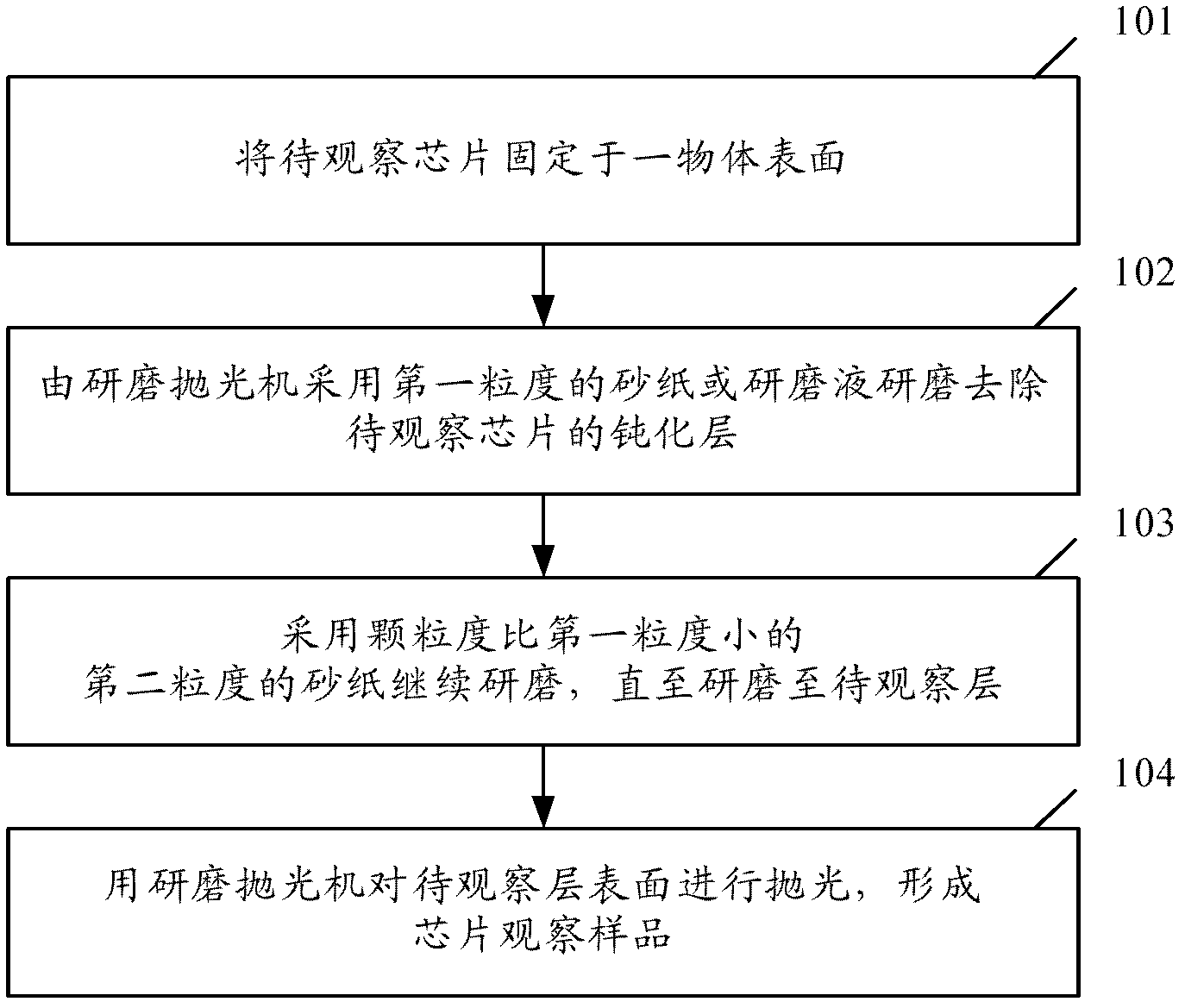
[0017] In order to avoid the use of complex and precise equipment such as R1E to form chip observation samples, reduce implementation complexity, improve efficiency, reduce costs, and improve the general applicability of making chip observation samples, an embodiment of the present invention provides a method for making chip observation samples And system.

[0018] The preferred embodiments of the present invention will be described in detail below with reference to the accompanying drawings.

[0019] In the embodiment of the present invention, the chip observation sample making system mainly includes the chip to be observed, a fixed object, and a grinding and polishing machine. Among them,

[0020] Fixed object, used to fix the chip to be observed on its surface;

[0021] Grinding and polishing machine, used to grind and remove the passivation layer of the chip to be observed with sandpaper of the first particle size or grinding fluid, and continue to grind with sandpaper of the seco...


PUM


Abstract

The invention discloses a chip observation sample manufacture method and a system. The chip observation sample manufacture method and the system are used for forming a chip observation sample without using a reactive ion etching (RIE) device, and are capable of reducing realization complexity, improving efficiency, reducing cost and improving general applicability in manufacturing the chip observation sample. The chip observation sample manufacture method comprises the following steps. A to-be-observed chip is fixed on the surface of an object, a passivation layer of the to-be-observed chip is ground through a grinding and polishing machine by utilizing sand paper with first granularity or grinding liquid, and grinding is performed by utilizing sand paper with second granularity which is smaller than the first granularity till a to-be-observed layer occurs. The grinding and polishing machine polishes the surface of the to-be-observed layer, and the chip observation sample is formed.

Description

Technical field [0001] The invention relates to the technical field of semiconductor production, and in particular to a method and system for manufacturing a chip observation sample. Background technique [0002] Observing the topography of each layer of a chip is a commonly used method to determine the internal structure of a chip. It is widely used in semiconductor production, testing and other fields, and can provide support for product production, improvement, and analysis. [0003] At present, in the process of chip production or testing, such as product failure analysis, process improvement, new product development, raw material evaluation, and reverse design, it is necessary to observe the structure of certain key layers of the chip. The thickness is very thin, about one thousandth of a millimeter, and it is tightly wrapped by a dielectric layer. Only reactive ion etching (Reactive Ion Etching, RIE) can form the observation surface of each key layer of the chip, but the RIE ...

Claims


Application Information

Patent Timeline
Patent Type & Authority Applications(China)
IPC IPC(8): H01L21/66G01N1/32
Inventor 金波
Owner FOUNDER MICROELECTRONICS INT
Why Eureka
Try Eureka