Semiconductor packaging piece, prefabricated lead frame and manufacturing method thereof

A semiconductor and packaging technology, which is applied in the field of square flat and no-lead semiconductor packages and its manufacturing method, can solve the problems of easily overflowing glue contaminating the bottom surface of the lead, poor coplanarity of the lead, and shedding of the plating layer, etc. Achieve the effect of improving reliability, reworkability, and reworkability

Inactive Publication Date: 2013-05-15
SILICONWARE PRECISION IND CO LTD
View PDF8 Cites 6 Cited by
  • Summary
  • Abstract
  • Description
  • Claims
  • Application Information

AI Technical Summary

Problems solved by technology

However, when this type of package is formed into the encapsulant, it is easy to overflow the glue and pollute the bottom surface of the lead. After forming the encapsulant, thermal stress will remain in the encapsulant, and after the singulation process, it will cause burrs on the outer edge of the lead. When the distance between the guide pins is too small, it is easy to contact with the adjacent guide pins and cause a short circuit
[0006] On the other hand, Japanese Patent No. 11-251505, Japanese Patent No. 09-312355, Japanese Patent No. 2001-024135, and Japanese Patent No. 2005-317998 have developed a square flat non-guide pin whose guide pin protrudes from the bottom surface of the encapsulant. However, when the package needs to be reworked after soldering the external device, after the package is removed from the printed circuit board, it usually results in poor coplanarity of the leads or plating on the leads shedding problem
Therefore, the package that needs to be reworked cannot be reused after reprocessing

Method used


Image

  • Semiconductor packaging piece, prefabricated lead frame and manufacturing method thereof
  • Semiconductor packaging piece, prefabricated lead frame and manufacturing method thereof
  • Semiconductor packaging piece, prefabricated lead frame and manufacturing method thereof

Examples


Embodiment Construction

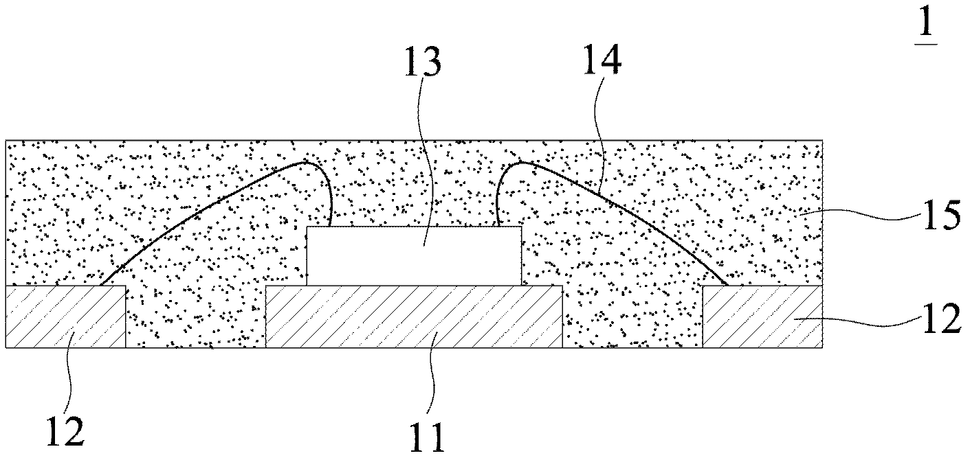
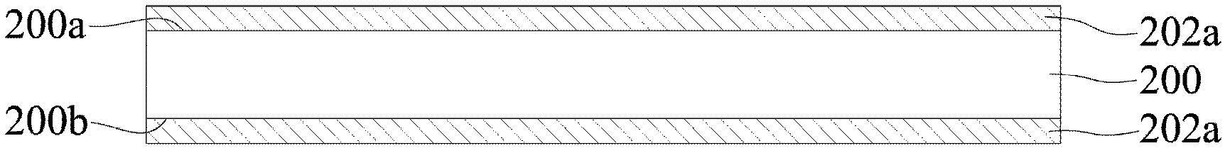
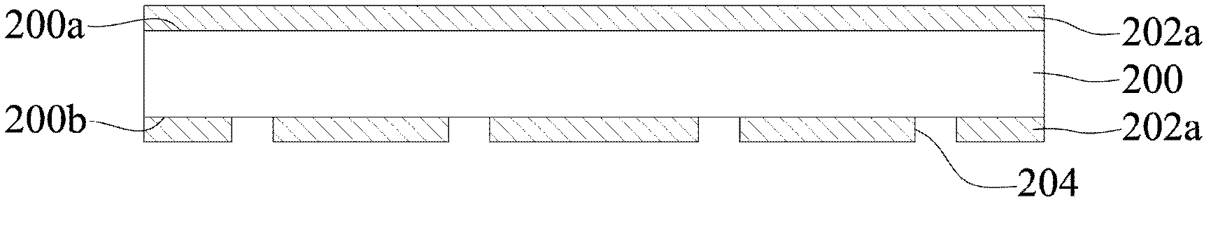
[0047]The implementation of the present invention will be described below through specific examples, and those skilled in the art can easily understand other advantages and effects of the present invention from the content disclosed in this specification. The present invention can also be implemented or applied through other different specific examples, and various modifications and changes can be made to the details in the present invention based on different viewpoints and applications without departing from the spirit of the present invention.

[0048] It should be noted that the structures, proportions, sizes, etc. shown in the drawings attached to this specification are only used to match the content disclosed in the specification for the understanding and reading of those skilled in the art, and are not intended to limit the implementation of the present invention. Limiting conditions, so there is no technical substantive meaning, any modification of structure, change of ...


PUM


Abstract

The invention provides a semiconductor packaging piece, a prefabricated lead frame and a manufacturing method thereof. The semiconductor packaging piece comprises packaging colloid; a plurality of guide pins partially embedded into the packaging colloid; surface processing layers formed on the top surface, the bottom surface and the recess of each guide pin; and a semiconductor chip embedded in the packaging colloid and used for being electrically connected with the guide pins.

Description

technical field [0001] The invention relates to a semiconductor package and a manufacturing method thereof, in particular to a quad-flat non-leaded (QFN) semiconductor package and a manufacturing method thereof. Background technique [0002] With the rapid development of semiconductor technology, various packaging structures have been developed for semiconductor devices, and the semiconductor device mainly uses a lead frame (Lead Frame) as a chip carrier to form a semiconductor package. The lead frame includes a chip seat and a plurality of leads formed around the chip seat, the semiconductor chip is bonded to the chip seat, and the chip is electrically connected to the plurality of leads with bonding wires, and then covered by encapsulant The chip, the chip seat, the bonding wire and the plurality of leads form the semiconductor package of the lead frame. [0003] In addition, there are many types and types of semiconductor packages with lead frames, for example, quad-flat...

Claims


Application Information

Patent Timeline
Patent Type & Authority Applications(China)
IPC IPC(8): H01L23/31H01L23/495H01L21/60
CPCH01L24/97H01L2924/15311H01L2224/97H01L2224/16245H01L2224/73265H01L2224/32245H01L2224/48247H01L24/73H01L2924/181H01L2224/81H01L2224/85H01L2924/00012H01L2924/00
Inventor 孙铭成洪良易萧惟中白裕呈林俊贤郭丰铭江东昇
Owner SILICONWARE PRECISION IND CO LTD
Why Eureka
Try Eureka