Production method of multilayer printed circuit board

A technology of printed circuit boards and manufacturing methods, which is applied in the direction of multilayer circuit manufacturing, etc., can solve problems such as poor flatness of multilayer printed circuit boards, explosive boards, and thickness differences of finished products, so as to improve manufacturing yield and Uniformity of line width, reduction of board warpage, and improvement of inner layer flatness

Inactive Publication Date: 2013-05-22
明光瑞智电子科技有限公司
View PDF5 Cites 7 Cited by
  • Summary
  • Abstract
  • Description
  • Claims
  • Application Information

AI Technical Summary

Problems solved by technology

[0003] The purpose of the present invention is to make up for the defects of the prior art, and to provide a multilayer printed circuit board that can effectively solve the problems of poor flatness, explosive boards, and large differences in thickness of finished products in the production process of multilayer printed circuit boards. How to make a circuit board

Method used


Image

  • Production method of multilayer printed circuit board
  • Production method of multilayer printed circuit board

Examples


Embodiment Construction

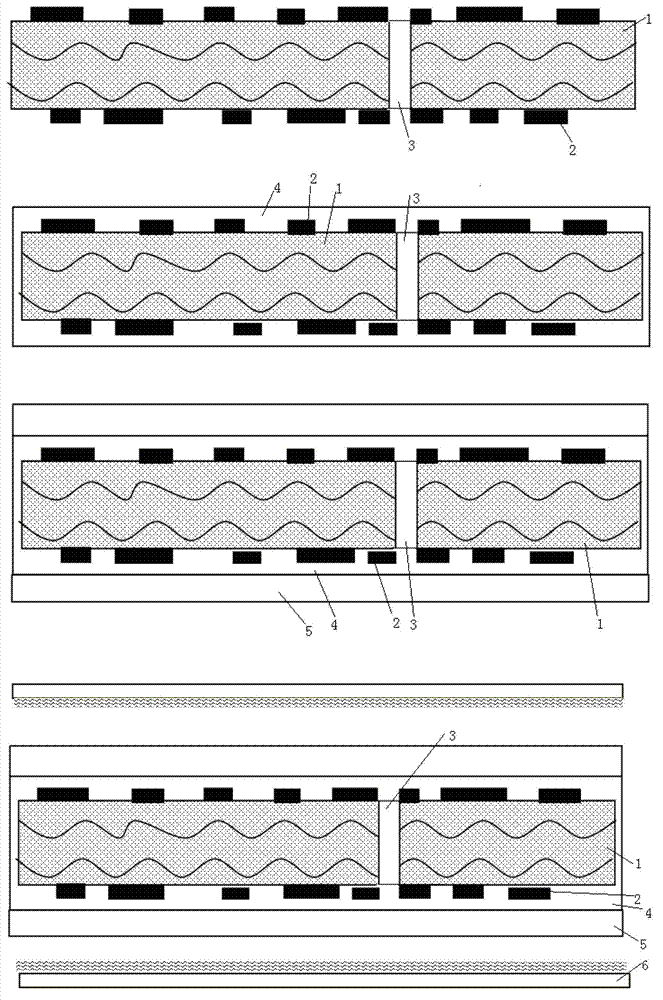
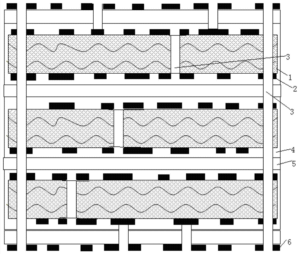
[0018] Such as figure 1 As shown, a manufacturing method of a multilayer printed circuit board is characterized in that it comprises the following steps:

[0019] (1) A layer of copper foil wiring layer 2 is respectively arranged on the upper and lower sides of the copper-clad substrate or insulating board 1, and circuit vias 3 are arranged between the layers to connect the upper and lower sides;

[0020] (2) After the circuit of the copper-clad substrate or insulating board 1 is completed, carry out black-browning treatment, and then put it into the epoxy resin tank with circulating control temperature, humidity and solid content ratio, and attach a layer of epoxy resin Glue 4 and fully cured;

[0021] (3) Then attach a thin layer of epoxy resin glue 5 to the copper-clad substrate or insulating board 1 and bake it to a semi-cured state;

[0022] (4) Laying a plurality of the copper-clad substrates or insulating boards 1 together, and laying the copper foil 6 on top and bottom, and t...


PUM


Abstract

The invention discloses a production method of a multilayer printed circuit board. Two copper foil wire layers are disposed on upper and lower surfaces of a copper-clad substrate or insulating plate respectively, and circuit through holes by which the upper and lower surface are communicated are established between the layers. After wiring on the copper-clad substrate or insulating plate is complete, oxidation is performed and the copper-clad substrate or insulating plate is placed in an epoxy resin glue cell for cycle control of temperature, humidity and solid-content ratio. The copper-clad substrate or insulating plate is coated with an epoxy resin glue layer. After the epoxy resin glue layer fully solidifies, an epoxy resin thin glue layer is applied to the copper-clad substrate or insulating plate and is baked to semi-solid state. Multiple copper-clad substrates or insulating plates are stacked. After copper foils are spread to the top and bottom of the stack, the stack is subjected to high-temperature press-fitting. The press-fitted copper-clad substrates or insulating plates are subjected to surface circuit treatment, and circuit through holes are established between the plates to allow for communication of circuits in all layers. Flatness of the inner layer of the printed circuit board is improved, inner buried holes are smoothed, manufacturing yield of fine lines and uniformity of line width are improved, and bending and warping degree of the printed circuit board is lowered.

Description

Technical field [0001] The invention relates to a production process of a PCB build-up method, in particular to a manufacturing method of a multilayer printed circuit board. Background technique [0002] Due to the rapid progress of volume circuits, such as the speed of volume circuits, the reduction of area, and the increase in heat dissipation requirements, they immediately impact the packaging technology of volume circuits. Nowadays, the new packaging technology and the market demand for lightness, thinness, and small size have also impacted The technology of multi-layer boards, which is currently commonly known as High Density Interconnection (HDI) Printed Circuit Board (PCB), is aimed at high-density, fine-line, and blind-buried vias. The difficulty of controlling the thickness of the board and the difficulty of filling the blind and buried holes is an important topic at present. In order to solve this difficulty, a high-reliability Epoxy Resin Thin Core technology prod...

Claims


Application Information

Patent Timeline
Patent Type & Authority Applications(China)
IPC IPC(8): H05K3/46
Inventor 袁燕华陈建福
Owner 明光瑞智电子科技有限公司
Why Eureka
Try Eureka