Silver bond wire for semiconductor devices

A bonding wire and semiconductor technology, applied in the field of bonding wire, can solve problems such as cost reduction, functional degradation, and unusability

Inactive Publication Date: 2013-06-05
赫劳斯材料工艺有限及两合公司
View PDF7 Cites 17 Cited by
  • Summary
  • Abstract
  • Description
  • Claims
  • Application Information

AI Technical Summary

Problems solved by technology

[0004] However, there is a limit in cost reduction because a large amount of gold (Au) is contained in the gold (Au)-silver (Ag) alloy wire
In addition, copper wires and copper wires coated with palladium (Pd) cannot be used for LED packages because reflectivity, the most important function of LEDs, is deteriorated

Method used


Image

  • Silver bond wire for semiconductor devices
  • Silver bond wire for semiconductor devices
  • Silver bond wire for semiconductor devices

Examples


Embodiment Construction

[0016] The advantages and characteristics of the present invention and methods for obtaining them will be more apparent from the ensuing embodiments in conjunction with the accompanying drawings. However, the present invention is not limited to the disclosed embodiments and can be implemented in various ways. The embodiments are provided to complete the disclosure of the present invention and to allow those skilled in the art to fully understand the scope of the present invention. The invention is defined by the claims. The same reference numerals refer to the same or similar parts throughout the drawings.

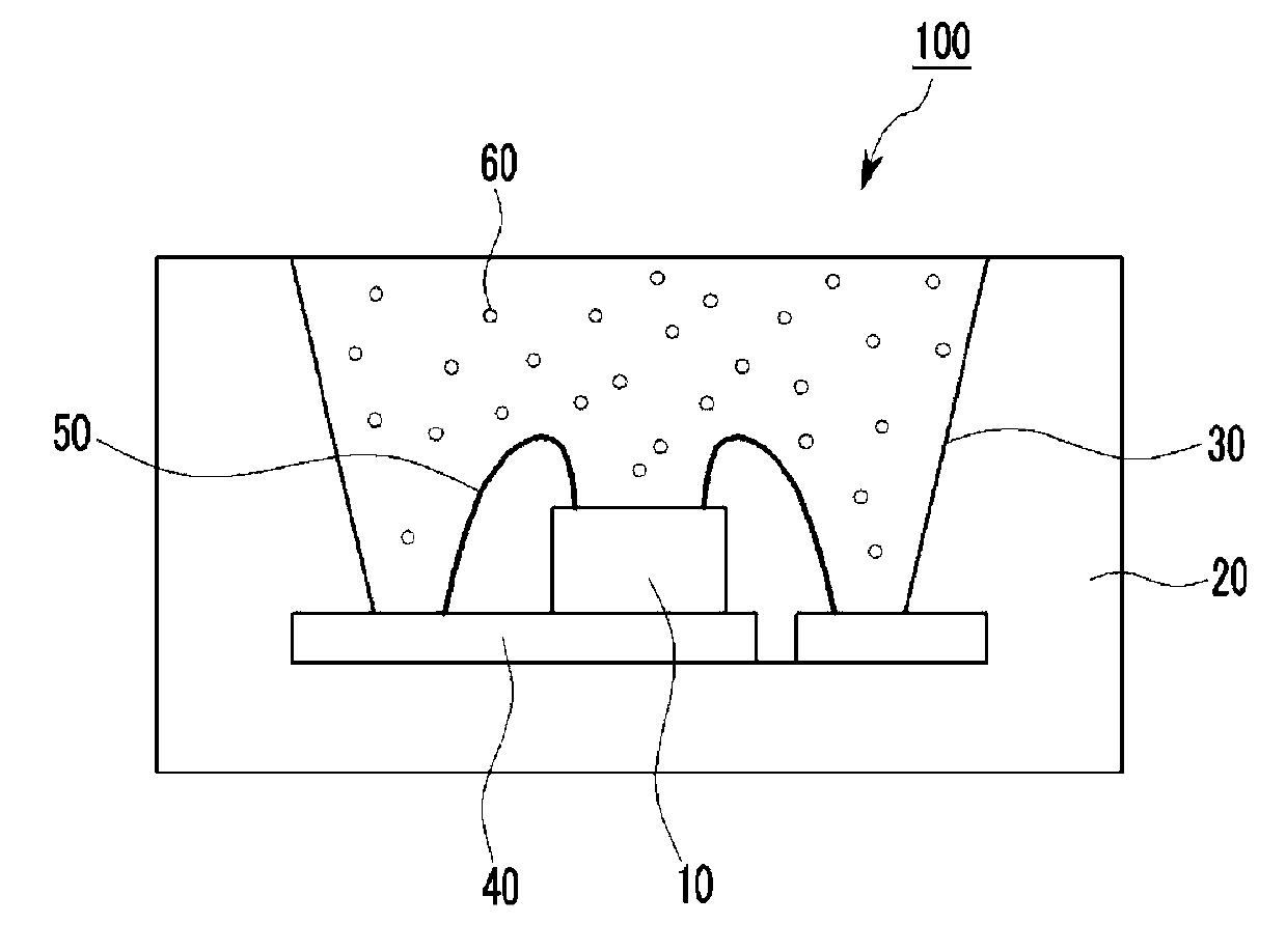
[0017] A bonding wire of a semiconductor device according to an exemplary embodiment of the present invention is described in detail below with reference to the accompanying drawings. For reference, in describing the present invention, a detailed description of known functions and constructions will be omitted if it is considered to make the gist of the present invention...


PUM

PropertyMeasurementUnit
diameteraaaaaaaaaa

Abstract

A bonding wire for semiconductor devices and a method of manufacturing the same are disclosed. The bonding wire for semiconductor devices according to the present invention includes at least one selected from the group consisting of zinc (Zn), tin (Sn), and nickel (Ni) at 5 ppm to 10 wt%, and the remainder including silver (Ag) and other inevitable impurities.

Description

technical field [0001] The present invention relates to a bonding wire, and more particularly, to a bonding wire for a semiconductor device and a light emitting diode (LED) package using the bonding wire, in which silver (Ag) is used as a main component. Background technique [0002] A bonding wire is a metal wire for electrically connecting an IC chip or an LED chip and a lead frame, and is generally composed of gold (Au). [0003] In order to reduce costs when manufacturing bonding wires, copper (Cu) wires or copper (Cu) wires with palladium (Pd) coated thereon have been tried for bonding wires due to the sudden increase in the price of gold (Au) worldwide recently. . Copper (Cu) wires are mass-produced by some manufacturers, but research on gold (Au)-based alloy wires is ongoing because the properties of copper (Cu) are not close to those of gold (Au). Research has been conducted on gold (Au)-silver (Ag) alloy wires as gold (Au)-based alloy wires. The gold (Au)-silver ...

Claims


Application Information

Patent Timeline
Patent Type & Authority Applications(China)
IPC IPC(8): C22C5/06C22C5/08H01L33/62
CPCH01L24/43C22C5/08H01L24/48H01L2224/45139H01L2924/12041H01L2224/43H01L2224/45565H01L2224/48247H01L24/45H01L2924/00015H01L2924/01029B21C3/00H01L2924/01028H01L2224/45144C22C5/06H01L33/62H01L2924/01012H01L2224/48091H01L2924/01013H01L2224/45147H01L2224/45015H01L2224/43848H01L2924/01015H01L2924/01006H01L2924/01047H01L2924/181H01L2924/00011H01L2224/48257H01L2924/0103H01L2924/0105H01L2924/01078H01L2924/01076H01L2924/01079H01L2924/01046H01L2924/01004H01L2924/01057H01L2924/01039H01L2924/0102H01L2924/01056H01L2924/01058H01L2224/45664H01L2924/01204H01L2924/01045H01L2924/013H01L2924/00013H01L2924/00014H01L2924/00H01L2924/00012H01L2924/01049
Inventor E-K·郑J-S·柳Y-D·卓
Owner 赫劳斯材料工艺有限及两合公司
Why Eureka
Try Eureka