

Automatic wiring method of integrated circuit layout after lessening experiment
An integrated circuit and wiring technology, applied in the field of integrated circuit layout processing, can solve the problems of inability to wire, easy to make mistakes, take a long time, etc., to achieve the effect of fast automatic connection and speed up
- Summary
- Abstract
- Description
- Claims
- Application Information
AI Technical Summary
Problems solved by technology
Method used
Image

Examples
Embodiment Construction
[0042] The method for automatic connection of the integrated circuit layout of the present invention after the reduction experiment comprises the following steps:
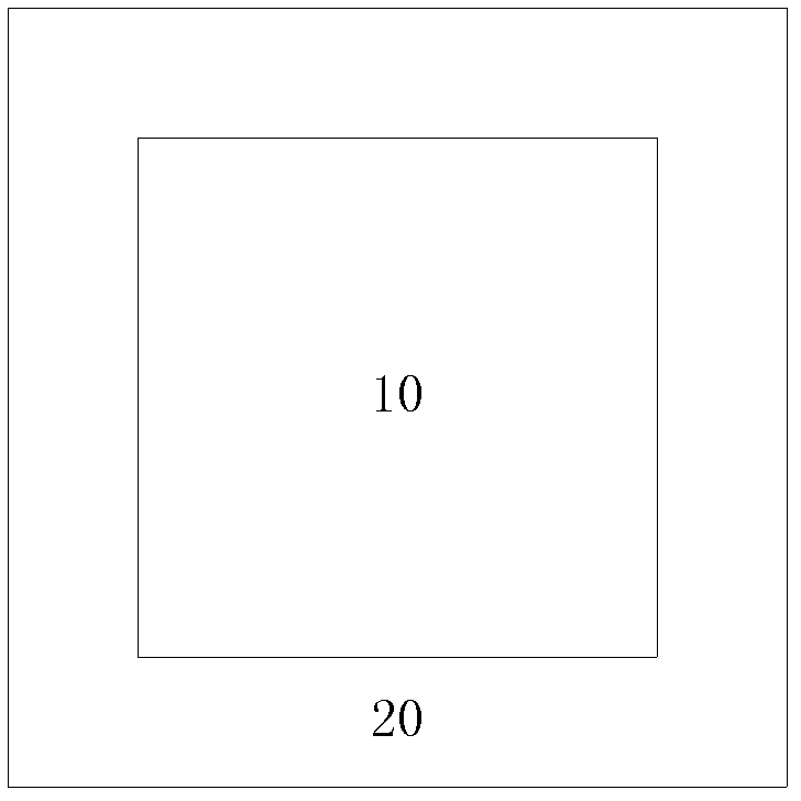
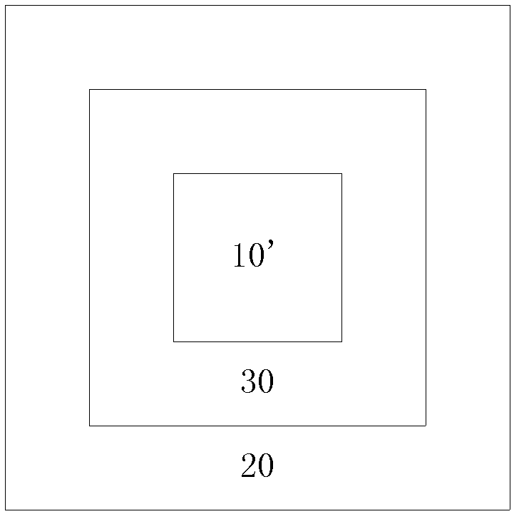
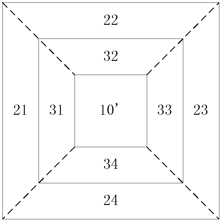
[0043] In the first step, the reduced cell array 10' is simply referred to as the reduced array 10'.
[0044] see Figure 1c , the peripheral circuit 20 is divided into four areas: upper, lower, left and right, which are respectively called the peripheral left area 21 , the peripheral upper area 22 , the peripheral right area 23 , and the peripheral lower area 24 .
[0045] The blank area 30 between the reduced array 10' and the peripheral circuit 20 is also divided into four areas: upper, lower, left and right, which are respectively called blank left area 31, blank upper area 32, blank right area 33, blank lower area 34.
[0046] Preferably, the reduced array 10 ′, the inner and outer rings of the peripheral circuit 20 , and the inner and outer rings of the blank area 30 are all rectangles on the layout, and th...
PUM
 Abstract
Description
Claims
Application Information