Manufacturing method and structure of fin field-effect transistor (FinFET) device

A manufacturing method and device technology, which can be used in semiconductor/solid-state device manufacturing, semiconductor devices, electrical components, etc., can solve problems such as the inability of FinFET devices to meet the requirements, and achieve the effects of simple manufacturing process, increased aspect ratio, and improved driving current.

Inactive Publication Date: 2013-06-05
SEMICON MFG INT (SHANGHAI) CORP
View PDF7 Cites 0 Cited by
  • Summary
  • Abstract
  • Description
  • Claims
  • Application Information

AI Technical Summary

Problems solved by technology

[0005] As the semiconductor industry advances to the 22nm technology node, the manufactured FinFET devices are required to have small

Method used


Image

  • Manufacturing method and structure of fin field-effect transistor (FinFET) device
  • Manufacturing method and structure of fin field-effect transistor (FinFET) device
  • Manufacturing method and structure of fin field-effect transistor (FinFET) device

Examples


Embodiment Construction

[0023] The manufacturing method of the FinFET device proposed by the present invention will be further described in detail below with reference to the drawings and specific embodiments.

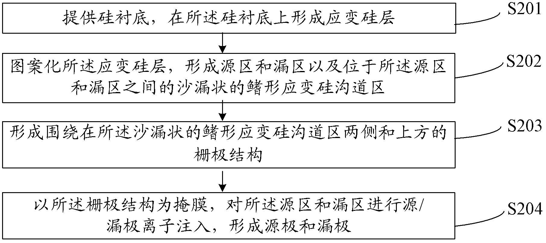
[0024] Such as figure 2 As shown, the present invention proposes a manufacturing method of a FinFET device, comprising:

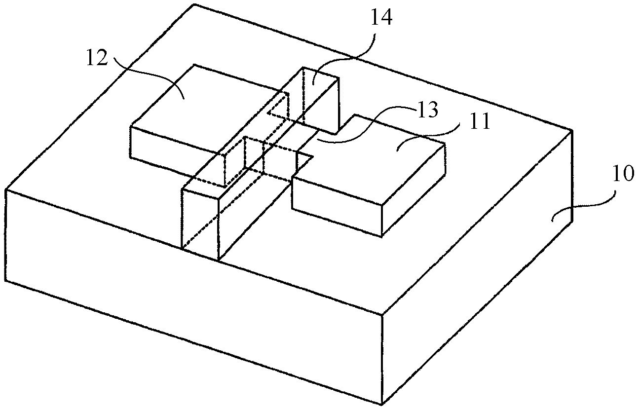
[0025] S201, providing a silicon substrate, and forming a strained silicon layer on the silicon substrate;

[0026] S202, patterning the strained silicon layer to form a source region and a drain region and an hourglass-shaped fin-shaped strained silicon channel region between the source region and the drain region;

[0027] S203, forming gate structures surrounding and above the hourglass-shaped fin-shaped strained silicon channel region;

[0028] S204. Using the gate structure as a mask, perform source / drain ion implantation on the source region and the drain region to form a source electrode and a drain electrode.

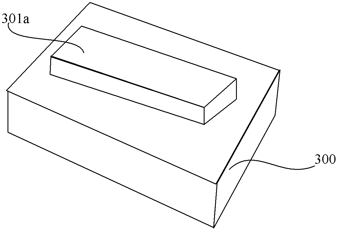
[0029] Attached below Figure 3A-3D right figur...


PUM


Abstract

The invention provides a manufacturing method and structure of a fin field-effect transistor (FinFET) device. A fin-shaped strained silicon channel region in an hourglass shape is adopted to replace a fin-shaped strained silicon channel region in a traditional rectangular or square shape, breadth-length ratio of a fin-shaped strained silicon channel is increased, driving current of the FinFET device is remarkably improved, and a manufacturing process is simple.

Description

technical field [0001] The invention relates to the field of semiconductor manufacturing, in particular to a manufacturing method and structure of a FinFET device. Background technique [0002] MOSFET (Metal Oxide Semiconductor Field Effect Transistor) is the main component of most semiconductor devices. When the channel length is less than 100nm, in the traditional MOSFET, the source and drain regions are separated by the semiconductor material of the silicon substrate surrounding the active region. Interaction, the distance between the drain and the source is also shortened, resulting in a short channel effect, so that the control ability of the gate to the channel becomes worse, and it becomes more and more difficult for the gate voltage to pinch off the channel The larger the , the easier it is for the subthrehhold leakage to occur. [0003] Fin field effect transistor (Fin Field effect transistor, FinFET) is a new metal oxide semiconductor field effect transistor, its ...

Claims


Application Information

Patent Timeline
IPC IPC(8): H01L21/336H01L21/28
Inventor 赵猛
Owner SEMICON MFG INT (SHANGHAI) CORP
Why Eureka
Try Eureka