Wafer structure for reducing damage of wafer cutting stress and layout design method

A wafer and graphics technology, applied in computing, special data processing applications, instruments, etc., can solve problems such as chip access and chip failure, and achieve the effect of preventing stress cracking and shortening the damage distance

Active Publication Date: 2013-06-05
HEJIAN TECH SUZHOU
View PDF6 Cites 5 Cited by
  • Summary
  • Abstract
  • Description
  • Claims
  • Application Information

AI Technical Summary

Problems solved by technology

In the case of serious stress damage, the chip seal ring can be damaged and enter the inside of the chip, directly causing the chip to fail

Method used


Image

  • Wafer structure for reducing damage of wafer cutting stress and layout design method
  • Wafer structure for reducing damage of wafer cutting stress and layout design method
  • Wafer structure for reducing damage of wafer cutting stress and layout design method

Examples


Embodiment Construction

[0039] In order to make the purpose, technical solution and advantages of the present invention clearer, the present invention will be further described in detail below in conjunction with the accompanying drawings and embodiments. The specific embodiments described here are only used to explain the present invention, but not to limit the present invention.

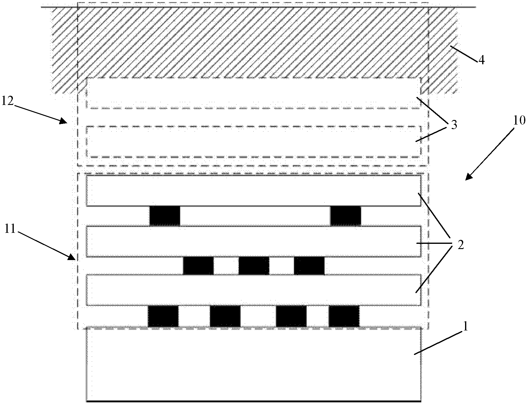
[0040] The present invention provides a wafer structure that alleviates wafer cutting stress damage, such as image 3 As shown, the wafer structure 10 includes a high-density metal layer and an oxide passivation protection layer thereon. The oxide passivation protection layer includes a metal layer 3 without pattern connection and a metal layer 3 without pattern connection The upper polishing pad layer 4; the wafer structure also includes a window 5 and a metal dummy device 6, the window 5 is arranged on the oxide passivation protection layer above the feature pattern of the wafer structure 10, and the metal dummy device ...


PUM


Abstract

The invention discloses a wafer structure for reducing damage of wafer cutting stress and a layout design method. The wafer structure comprises a high-density metal layer and an oxide passivation protection layer which is located above the high-density metal layer. The oxide passivation protection layer comprises a metal layer without graph connecting lines and a grinding cushion layer which is located above the metal layer without the graph connecting lines. The wafer structure further comprises an opening window and a metal fake component, wherein the opening window is arranged on the oxide passivation protection layer above characteristic graphs of the wafer structure, and the metal fake component is arranged on the metal layer without the graph connecting lines. According to the wafer structure for reducing the damage of the wafer cutting stress and the layout design method, large-energy stress crack is prevented from occurring when a wafer is cut, or a damage distance of the crack is shortened.

Description

technical field [0001] The invention relates to the field of semiconductor manufacturing, in particular to a wafer structure and layout design method for alleviating wafer cutting stress damage. Background technique [0002] In the existing CMOS process, when the pattern density of the layout (layout) in the dicing line, especially the density of the metal via / contact (MVIA / CONT) layer is high, and the area is large, when the chip is cut, it is easy to be caused by high Density of the metal connection gathers, resulting in a large area of ​​severe cracking during cutting, and at the same time causing a greater degree of cracking to the upper passivation protection layer (passivation). The stress failure can even break the chip protection ring (seal ring), and enter the customer chip, causing the chip to fail. This effect becomes more severe the closer to the corners of the chip. [0003] At present, there are two main methods commonly used in the industry to improve wafer ...

Claims


Application Information

Patent Timeline
IPC IPC(8): H01L23/00H01L27/02G06F17/50
Inventor 许喆洪文田张建伟
Owner HEJIAN TECH SUZHOU
Why Eureka
Try Eureka