Thin film transistor liquid crystal display device and repairing method thereof
A liquid crystal display device and thin film transistor technology, which is applied to instruments, nonlinear optics, optics, etc., can solve problems such as low repair success rate, and achieve the effects of avoiding short circuit phenomenon, avoiding light leakage, and improving repair success rate.
- Summary
- Abstract
- Description
- Claims
- Application Information
AI Technical Summary
Problems solved by technology
Method used
Image

Examples
Embodiment 1
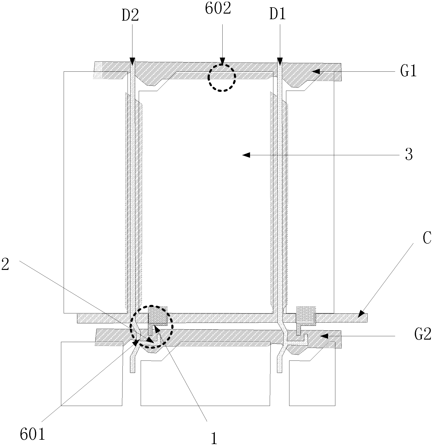
[0040] This embodiment discloses a thin film transistor liquid crystal display device, including:
[0041] Substrate, gate line, common line, gate insulating layer, silicon island, data line, source electrode, drain electrode, passivation layer and pixel electrode, described pixel electrode comprises the light-transmitting region of pixel electrode and the opaque region of pixel electrode In the light area, a repair mark is arranged on the gate line, and the repair mark corresponds to the overlapping part of the drain and the gate.
[0042] Specific settings such as Figure 4 Shown:
[0043] A substrate (not shown in the figure), the substrate is a glass substrate or a substrate of other materials.
[0044] The gate lines G11, G12 and the common line C11 are disposed on the first metal layer, and the first metal layer is disposed on the surface of the substrate.
[0045] Specifically, the common line C11 is U-shaped in each corresponding pixel area, and conducts through the...
Embodiment 2
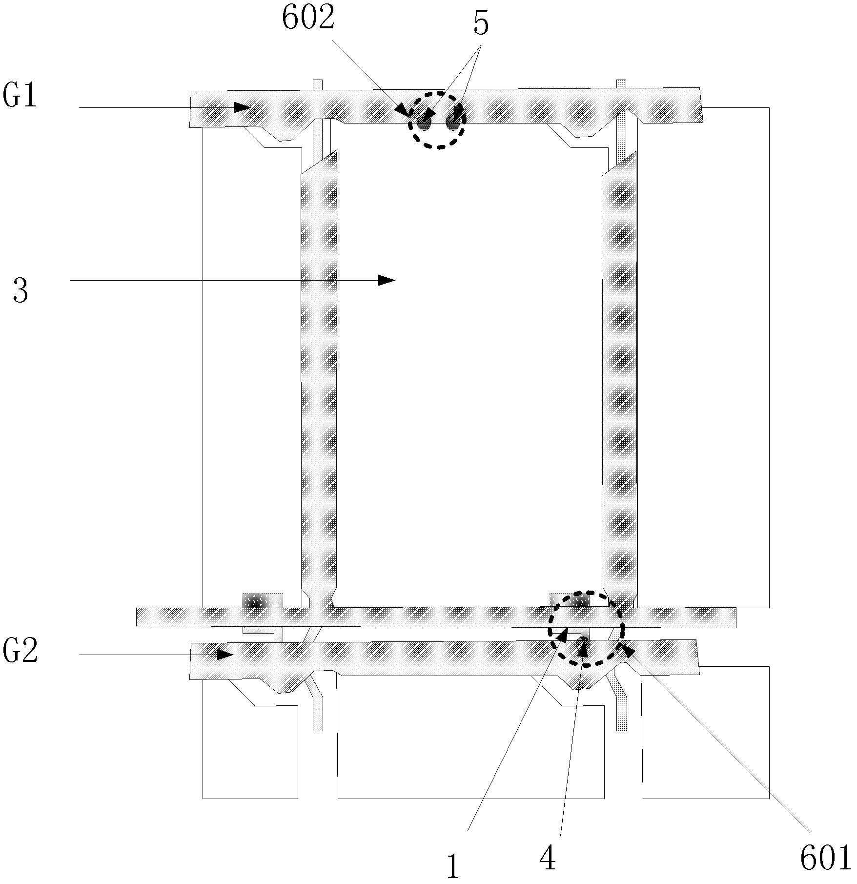
[0055] The difference between this embodiment and the first embodiment lies in that the repair mark corresponds to the opaque region of the pixel electrode, and a light-shielding structure is included between the gate insulating layer and the passivation layer corresponding to the repair mark.
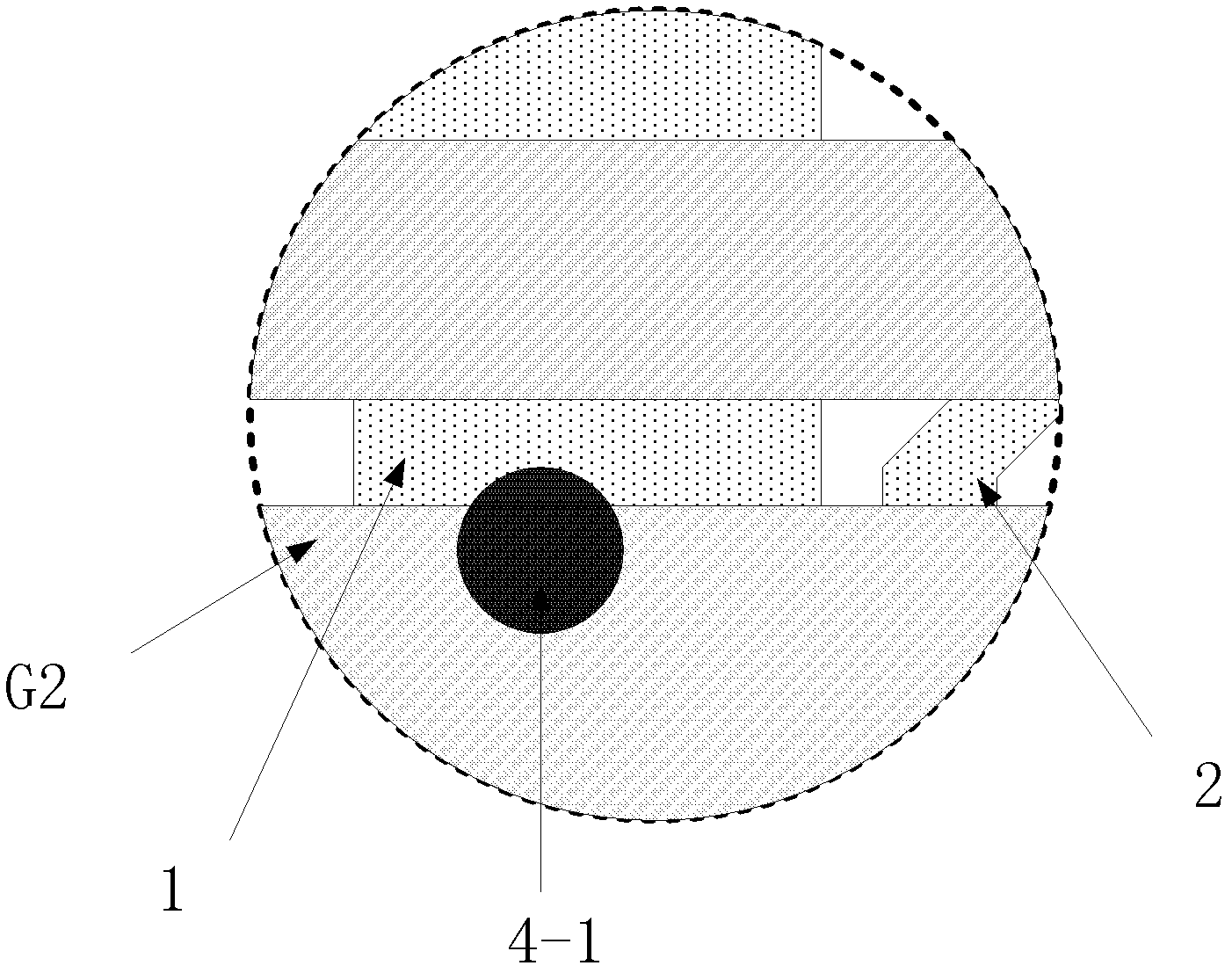
[0056] Such as Image 6 as shown, Image 6 -a is a top view, the repair mark X1 corresponds to the opaque area of the pixel electrode P11, and the repair mark X1 has a circular repair mark pattern that penetrates the gate line G11, that is, the laser can be used on the substrate side Welding technology welds the gate line G11 and the opaque area of the pixel electrode P11 together at the repair mark. Preferably, on the substrate side, laser welding technology can be used to weld the gate line G11 and the edge of the pixel electrode P11 at the repair mark. positions welded together, the repair mark figure can also be a rectangle or other figures that can play a marking role, and a ...
Embodiment 3
[0062] The difference between this embodiment and the above-mentioned embodiment is that, as Figure 7 As shown, the liquid crystal display device disclosed in this embodiment includes a first repair mark X11 and a second repair mark X12, and a light-shielding structure is included between the gate insulating layer and the passivation layer corresponding to the second repair mark X12.
[0063] The first repair mark X11 is the same as the repair mark X in the first embodiment, and the repair mark X12 is the same as the repair mark X1 in the second embodiment.
[0064] It can be seen that in the process of repairing bright spots of TFT liquid crystal display devices, the position of the repair point can be accurately judged, so as to avoid the short circuit between the gate line G12 and the source S11, improve the success rate of repair, and avoid pixel edge damage. The phenomenon of light leakage occurs, and since the gate insulating layer corresponding to the second repair mar...
PUM
 Abstract
Description
Claims
Application Information
 - R&D
- Intellectual Property
- Life Sciences
- Materials
- Tech Scout
- Unparalleled Data Quality
- Higher Quality Content
- 60% Fewer Hallucinations
Browse by: Latest US Patents, China's latest patents, Technical Efficacy Thesaurus, Application Domain, Technology Topic, Popular Technical Reports.
© 2025 PatSnap. All rights reserved.Legal|Privacy policy|Modern Slavery Act Transparency Statement|Sitemap|About US| Contact US: help@patsnap.com