Thick film circuit board and manufacturing method thereof

A technology of thick film circuit and manufacturing method, which is applied in the direction of printed circuit components, conductive pattern formation, containing printed electrical components, etc., can solve the problems of poor output voltage consistency, short service life, and poor linearity of output voltage, etc., to achieve Improve the wear-resistant working life, improve symmetry and linearity, and improve the effect of wear-resistant life

Active Publication Date: 2013-06-12
东莞市东思电子技术有限公司
View PDF4 Cites 3 Cited by
  • Summary
  • Abstract
  • Description
  • Claims
  • Application Information

AI Technical Summary

Problems solved by technology

[0016] The purpose of the present invention is to solve the deficiencies of the prior art, and provide a thick film circuit board, which solves the problem

Method used


Image

  • Thick film circuit board and manufacturing method thereof
  • Thick film circuit board and manufacturing method thereof
  • Thick film circuit board and manufacturing method thereof

Examples


Embodiment 1

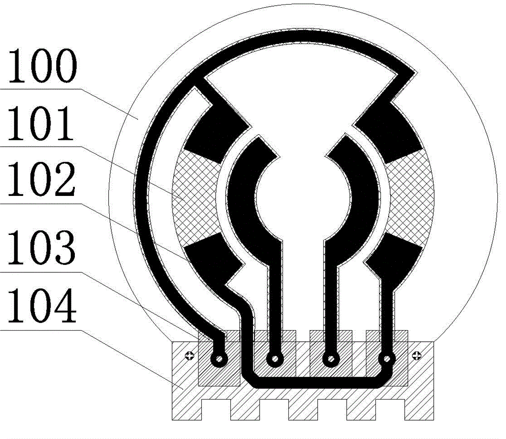
[0060] Example 1: see image 3 .

[0061] A thick film circuit board, comprising a PCB substrate 200, the PCB substrate 200 is provided with a front pad 201, a via hole 202 and a back pad 203, and the lower end of the front of the PCB substrate 200 is provided with a front insulating layer 204, And the lower end of the front pad 201 is located in the front insulating layer 204, the front side of the PCB substrate 200 is also provided with a front conductor circuit layer 205 connected to the upper end of the front solder pad 201, and the front conductor circuit layer 205 includes a first branch Line layer 23 and the second branch line layer 24, and the third branch line layer 25, the third branch line layer 25 is respectively connected with the first branch line layer 23 and the second branch line layer 24, and the front conductor line layer 205 is The silver-containing conductive paste is printed on the PCB substrate 200 and is a conductive layer with a thickness of less than...

Embodiment 2

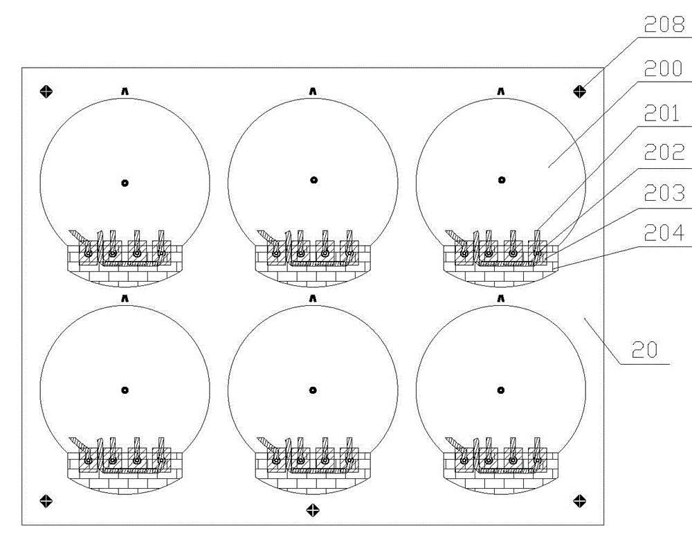
[0067] Example 2: see Figure 3 to Figure 7 .

[0068] A method for manufacturing a thick film circuit board, comprising the following steps:

[0069] Step 1 Through drilling, electroless copper deposition, yellow light lithography, etching, electroplating and other production processes, on the PCB substrate

[0070] A via hole 202, a front pad 201, a back pad 203, and a front insulating layer 204 are sequentially formed on the board 200

[0071] Wherein, the inner wall of the via hole 202 is provided with a conductive layer, and the conductive layer connects the front pad 201 and the back pad 203 .

[0072] The conductive layer of the via hole 202, the front pad 201, and the back pad 203 are sequentially formed with copper layer, nickel layer, and gold layer materials from the inside to the outside;

[0073] In the specific implementation, the copper layer is firstly covered with copper foil and bonded on the substrate, and then the copper layer is formed by masking, yello...


PUM

PropertyMeasurementUnit
Thicknessaaaaaaaaaa

Abstract

The invention relates to a thick film circuit board and a manufacturing method thereof. The thick film circuit board comprises a PCB (Printed Circuit Board) substrate, wherein the PCB substrate is provided with a front bonding pad, a via hole, a back bonding pad and a front insulating layer; the lower end of the front bonding pad is positioned in the front insulating layer; the front face of the PCB substrate is also provided with a front conductor circuit layer; the front conductor circuit layer comprises a first branch circuit layer, a second branch circuit layer and a third branch circuit layer and is a conductive layer with thickness of less than 10 mu m; and the middle part of the first branch circuit layer and the middle part of the second branch circuit layer are symmetrically provided with a first resistive layer and a second resistive layer respectively. The manufacturing method comprises the following steps of: forming the front bonding pad, the back bonding pad, the front insulating layer, the via hole, the front resistive layers and a bridging conductor on the PCB substrate through a thick film technology and punching. The front conductor circuit layer has small thickness, low resistive layer fall and a long service life; and by arranging a cut-off point, the resistive layer performance can be improved.

Description

technical field [0001] The invention relates to the technical field of thick-film circuit boards, in particular to a thick-film circuit board for electric power steering torque sensors and a manufacturing method thereof. Background technique [0002] Electric Power Steering (EPS for short) is a power steering system that directly relies on the motor to provide auxiliary torque. Compared with the traditional hydraulic power steering system HPS (Hydraulic Power Steering), the EPS system has low energy consumption and easy Convenience, high efficiency, good road feel, good return performance, compact structure, light weight, easy maintenance and other advantages. It is in line with the national industrial layout of new energy vehicles and energy-saving vehicles, conforms to the current development trend of low-carbon economy, and represents the development direction of automobile steering systems. [0003] Such as figure 1 As shown, the EPS is mainly composed of a torque sens...

Claims


Application Information

Patent Timeline
IPC IPC(8): H05K1/16H05K1/09H05K1/11H05K3/12
Inventor 邓进甫陈杏良
Owner 东莞市东思电子技术有限公司
Why Eureka
Try Eureka