Edge-emitting crystal laser with circular spot output and low divergence angle and composite waveguide device

A photonic crystal waveguide and composite waveguide technology, applied in the field of optical communication, can solve problems such as multi-mode lasing, affecting beam quality, etc., and achieve the effects of low circular spot output, increased stability, and high repeatability

Active Publication Date: 2013-06-19
INST OF SEMICONDUCTORS - CHINESE ACAD OF SCI
View PDF5 Cites 14 Cited by
  • Summary
  • Abstract
  • Description
  • Claims
  • Application Information

AI Technical Summary

Problems solved by technology

The output power of the laser can be increased by increasing the width of the waveguide, but too wide a strip width will cause multi-mode lasing and affect the beam quality

Method used


Image

  • Edge-emitting crystal laser with circular spot output and low divergence angle and composite waveguide device
  • Edge-emitting crystal laser with circular spot output and low divergence angle and composite waveguide device
  • Edge-emitting crystal laser with circular spot output and low divergence angle and composite waveguide device

Examples


Embodiment

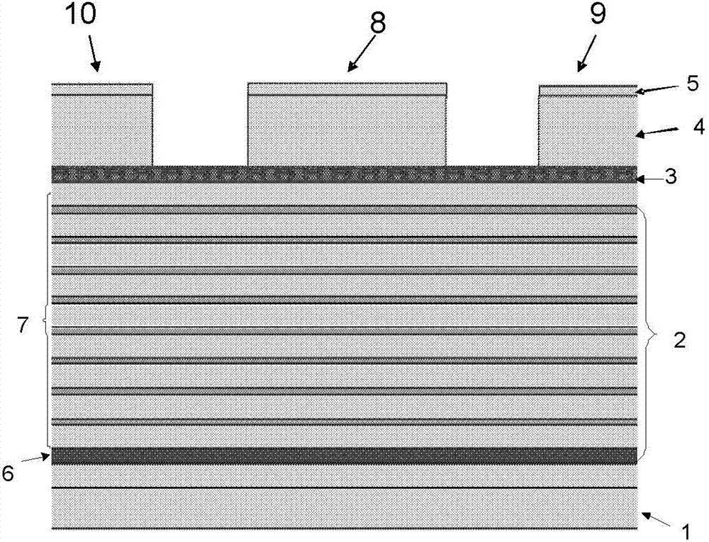
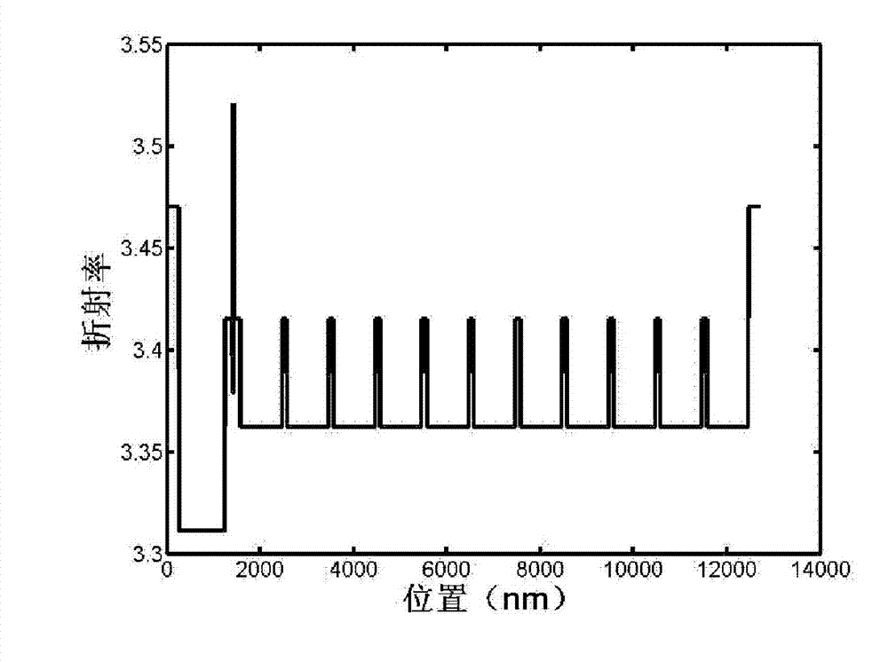
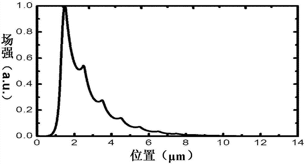
[0035] In a preferred example of the present invention, the loss modulation layer 6 and the mode expansion layer 7 in the vertically asymmetric photonic crystal waveguide structure are all n-type Al 0.1 GaAs / Al 0.2 GaAs, the thicknesses are 0.1 μm / 0.9 μm, the doping concentrations of layer 6 and layer 7 are different, and layer 6 is heavily doped. The substrate is N-type GaAs, and the active region is 3 pairs of continuously grown InGaAs / GaAsP quantum wells, and the refractive index of the GaAsP layer is lower than that of Al 0.2 The refractive index of GaAs has a gain peak near 1065nm in the infrared band. The upper confinement layer is p-type Al 0.3 GaAs, the thickness is 1μm, and the capping layer is P-type GaAs. The width of the ridge waveguide is 4 μm, and the etching depth reaches the first pair of quantum wells. The distance between the mesa and the ridge waveguide on both sides of the mode expansion region can be adjusted according to the distribution of the optica...


PUM


Abstract

The invention discloses a photonic crystal composted waveguide device used for improving the two dimension distant field morphology of an edge-emitting crystal laser. The structure is composed of a ridge waveguide structure which is parallel to heterogeneous section direction and an unsymmetrical photonic crystal structure which is vertical to heterogeneous section direction. The low divergence angle and the circular spot output are achieved by the combination of the ridge waveguide structure and the unsymmetrical photonic crystal structure. The vertical structure is an N-shaped substrate, an N-shaped photonic crystal waveguide, an active layer, a P-shaped limitation layer and a P-shaped cover layer in order from the bottom up, wherein the N-shaped photonic crystal waveguide is generated by the alternative development of materials with high refractive index and materials with low refractive index. Based on the adjusting function of photonic crystal to photo state, so that each of different model fields are provided with a different distribution of light fields and has distinguished property of space. Gain of model of a low-level model is maximized, so that stable emitting of the low-level model is achieved.

Description

technical field [0001] The invention relates to the field of optical communication, in particular to a circular spot output low-divergence angle edge-emitting photonic crystal laser and a composite waveguide device. Background technique [0002] With the development of optical communication, optical interconnection technology and various optoelectronic devices, laser technology has become an indispensable part of the development of modern science and technology. The application of lasers has covered various fields such as life, medicine, exploration, and national defense. With the continuous expansion of the application area, the types of lasers are also increasing. But cheap and reliable are prerequisites for a class of lasers to be popularized. In order to further meet the needs of industry and military, the improvement of semiconductor laser power and beam quality has become a research hotspot. For this reason, people have tried many structures and made a lot of efforts....

Claims


Application Information

Patent Timeline
Patent Type & Authority Applications(China)
IPC IPC(8): H01S5/22
Inventor 郑婉华张建心刘磊渠红伟张斯日古楞王海玲
Owner INST OF SEMICONDUCTORS - CHINESE ACAD OF SCI
Why Eureka
Try Eureka