USB (Universal Serial Bus) chip silicon wafer level automatic test device and test method

A technology of silicon wafer level and tester, which is applied in the field of USB chip silicon wafer level tester and USB chip silicon level tester, can solve the problems that the response signal processing of the USB chip cannot be realized, so as to reduce the test cost and improve the same test number, the effect of avoiding test errors

Active Publication Date: 2013-06-26
SHANGHAI HUAHONG GRACE SEMICON MFG CORP
View PDF7 Cites 5 Cited by
  • Summary
  • Abstract
  • Description
  • Claims
  • Application Information

AI Technical Summary

Problems solved by technology

Since the existing automatic tester cannot analyze the NRZI signal, even after the existing automatic tester reads the response signal of the USB chip, it cannot realize the processing of the response signal of the read USB chip

Method used


Image

  • USB (Universal Serial Bus) chip silicon wafer level automatic test device and test method
  • USB (Universal Serial Bus) chip silicon wafer level automatic test device and test method
  • USB (Universal Serial Bus) chip silicon wafer level automatic test device and test method

Examples


Embodiment Construction

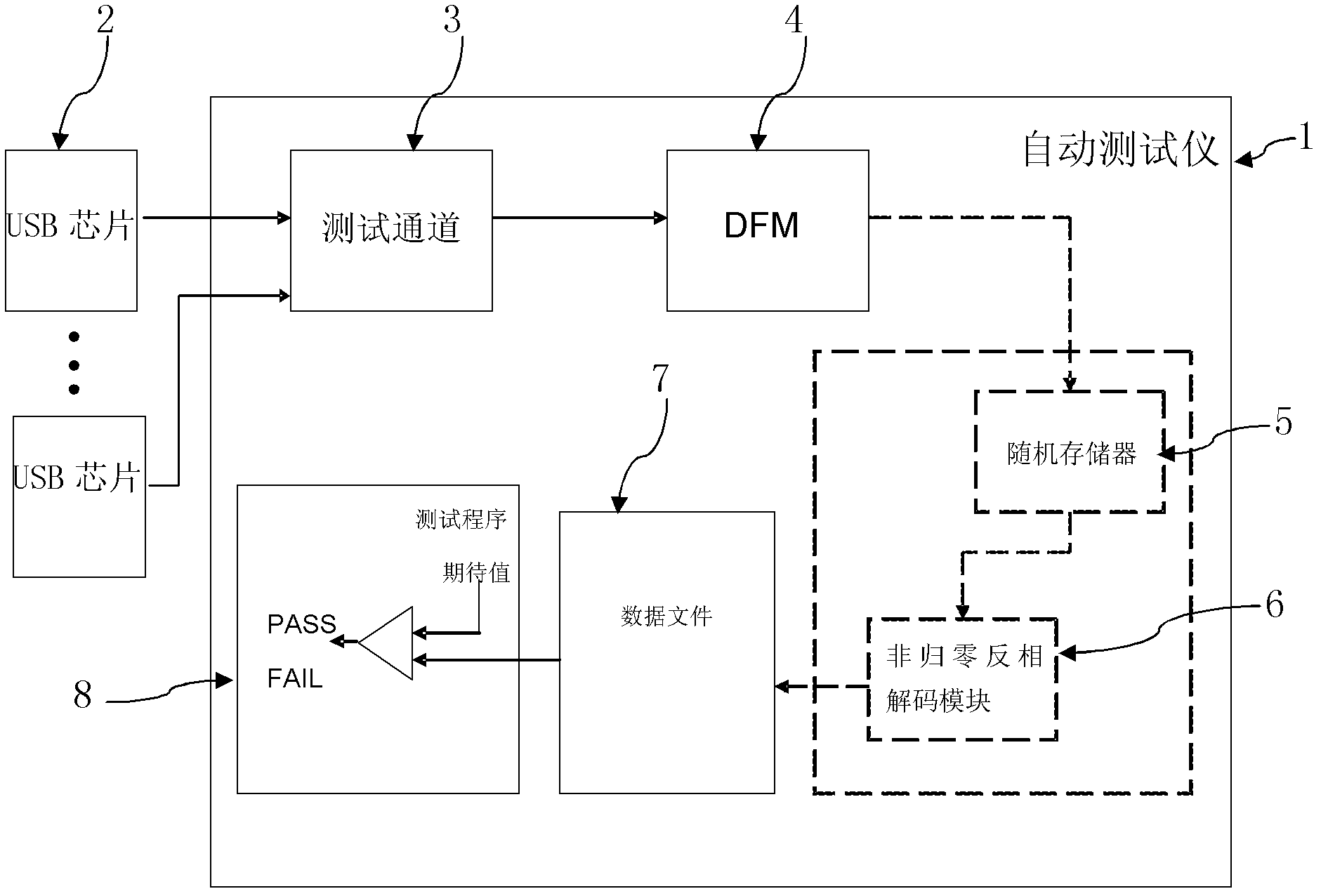
[0033] Such as image 3 As shown, it is a schematic diagram of a silicon-level automatic tester for a USB chip according to an embodiment of the present invention. The embodiment of the present invention USB chip silicon chip level automatic tester 1 is used for the silicon chip level test of USB chip 2, comprises: test channel 3, failure data memory 4, random access memory 5, non-return-to-zero inversion decoding module 6, data file 7 and test procedure 8.

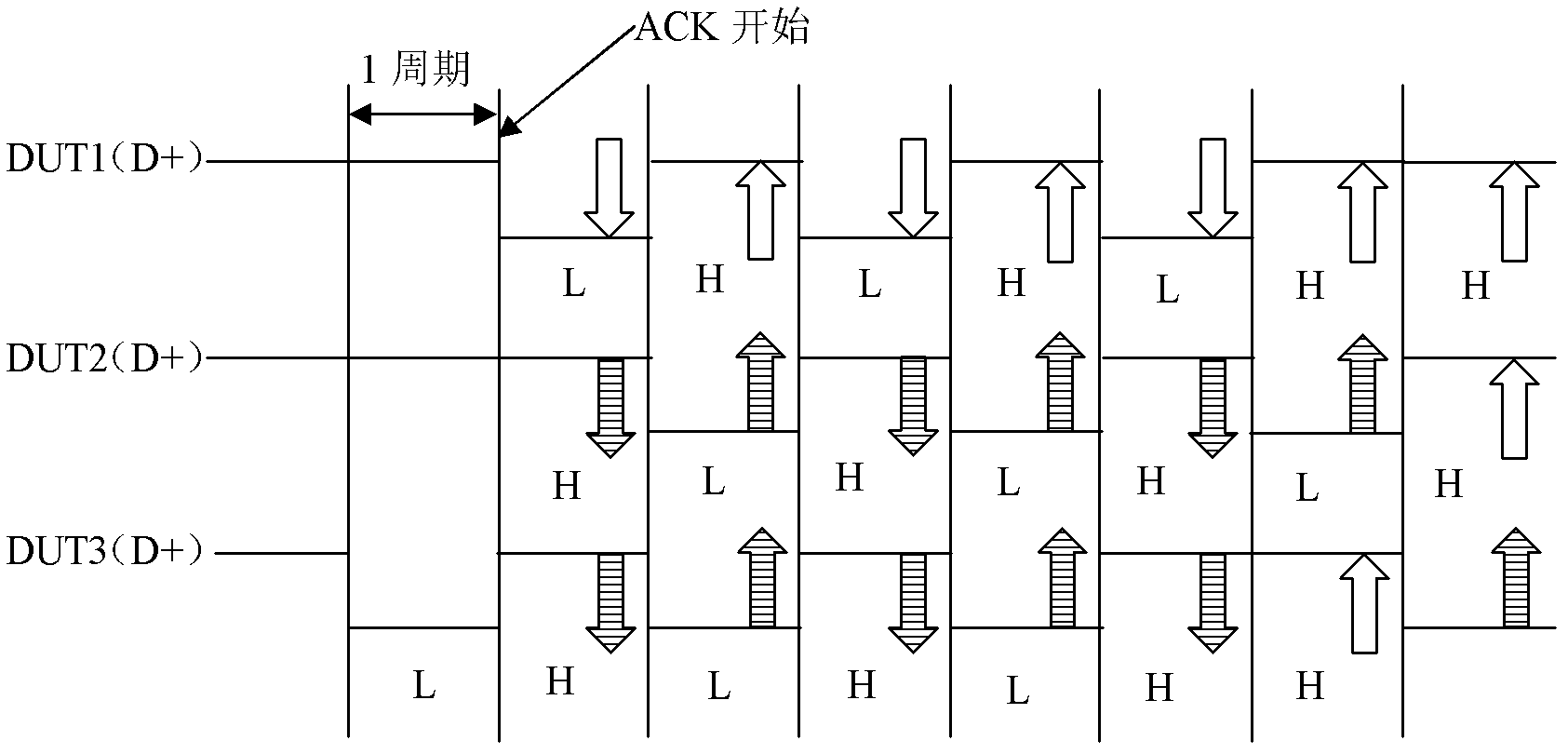
[0034] The test channel 3 includes multiple and is used to connect with one or more USB chips 2, wherein every two test channels are connected to one of the USB chips 2, and the test channel is used to receive each of the USB chips 2 The returned handshake response signal or data. The DP signal pin and the DM signal pin of each USB chip 2 are respectively connected to one of the test channels 3 . The handshake response signal or data handshake response signal includes ACK, NAK, STALL, and the data flow type of the hand...


PUM


Abstract

The invention discloses a USB chip silicon wafer level automatic test device which comprises a test channel, a failure data memory, a random access memory, a non-return-to-zero inverted decoding module, a data file and a test program. The USB chip silicon wafer level automatic test device can respectively store simultaneously-read handshake response signals or data of a plurality of USB chips in the random access memory to avoid test errors caused by the asynchronous response of the plurality of USB chips. The handshake response signals or data of the non-return-to-zero inverted coding, which are stored in the random access memory, can be decoded by the USB chip silicon wafer level automatic test device to achieve the simultaneous test of the plurality of USB chips, increase the number of simultaneously-tested chips and reduce the test cost. The invention also discloses a USB chip silicon wafer level automatic test method.

Description

technical field [0001] The invention relates to the field of semiconductor integrated circuit manufacturing, in particular to a USB chip silicon wafer level tester; the invention also relates to a USB chip silicon wafer level test method. Background technique [0002] Universal Serial Bus (Universal Serial Bus, USB) is a fast, bidirectional, synchronous, dynamically connected and inexpensive serial interface, which can meet the current and future needs of PC development. With the mass production of USB chips, the cost of testing continues to rise. [0003] In the existing method for testing USB chips at the silicon level, the testing device used is an Automated Test Equipment (ATE). The ATE is used as a transmitter, and the USB chip is used as a receiver. Real-time communication is performed between the ATE and the USB chip. As a signal transmitter, ATE is responsible for establishing tags and sending data; as a device under test (DUT), the USB chip will return a handshake ...

Claims


Application Information

Patent Timeline
Patent Type & Authority Applications(China)
IPC IPC(8): G01R31/28
Inventor 朱渊源
Owner SHANGHAI HUAHONG GRACE SEMICON MFG CORP
Why Eureka
Try Eureka