[0021] Embodiments of the present invention will be described below with reference to the drawings. Elements and features described in one drawing or one embodiment of the present invention may be combined with elements and features shown in one or more other drawings or embodiments. It should be noted that representation and description of components and processes that are not related to the present invention and known to those of ordinary skill in the art are omitted from the drawings and descriptions for the purpose of clarity.
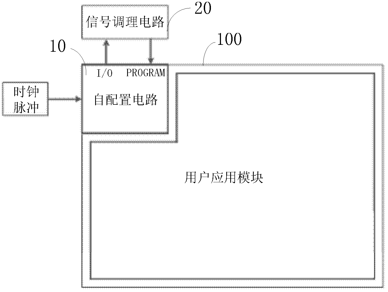
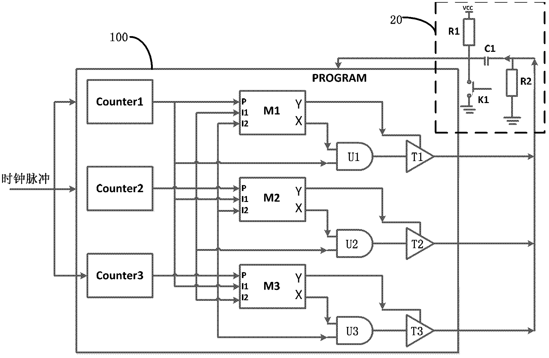
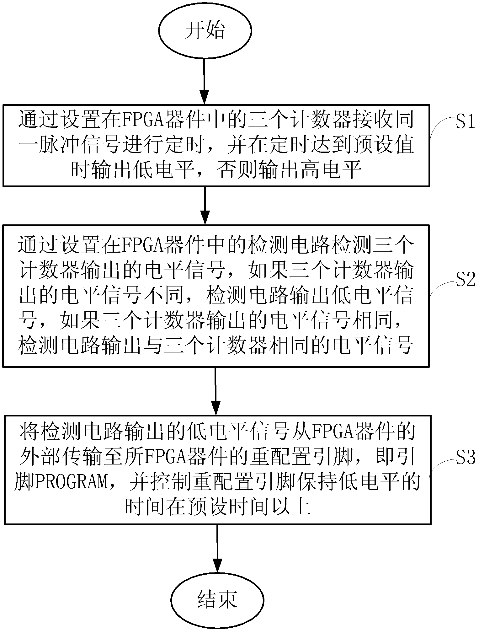
[0022] For SRAM-type FPGA devices, a reconfiguration pin is generally provided, and the FPGA device can enter the reconfiguration stage by applying a low-level pulse with a preset width to the pin. The invention provides an FPGA device self-weight configuration device. In the device of the present invention, the low-level pulse of the preset width is provided by the FPGA device to be configured, specifically, a self-configuration circuit is set in the FPGA device to be configured, and the output terminal of the self-configuration circuit is used as the FPGA device to be configured. An I/O pin of the device is connected to the reconfiguration pin through an external signal conditioning circuit. The self-configuration circuit can regularly output a reconfiguration signal or force a reconfiguration signal to be output when an error is detected. The reconfiguration signal is passed through the signal After conditioning, the conditioning circuit outputs to the reconfiguration pin of the FPGA device, so that the FPGA device enters the reconfiguration stage, and the signal conditioning circuit is used to control the reconfiguration pin to keep the low level longer than the preset time.
[0023] The present invention provides a self-reconfiguration device for an FPGA device, which includes a self-configuration circuit arranged in the FPGA device and a signal conditioning circuit arranged outside the FPGA device. The self-configuration circuit includes first to third counters and connections to the first to third counters. The detection circuit of the counter, the first to the third counters are used to receive the same clock pulse signal for timing, and output a low level signal when the timing reaches the preset value, otherwise output a high level signal, the detection circuit is used to detect the first Whether one of the third counters outputs a different level signal from the other two counters, and outputs a low level signal when it is detected to be different, and outputs the same level signal when it is detected that the first to third counters output the same level signal The level signals of the first to third counters are the same, the output end of the detection circuit is connected to the signal conditioning circuit, and the signal conditioning circuit is used to transmit the low level signal output by the detection circuit to the reconfiguration pin, and control the reconfiguration pin to maintain The time of low level is above the preset time.
[0024]Optionally, the detection circuit includes first to third voters, first to third operators, first to third tri-state gate circuits, each of the first to third voters has first to third input terminals and The first output end and the second output end, the output end of the first counter is connected to the first input end of the first voter, the second input end of the second voter and the second input end of the third voter, the second The output of the counter is connected to the first input of the second voter, the second input of the first voter and the third input of the third voter, and the output of the third counter is connected to the first input of the third voter Terminal, the third input terminal of the first voter and the third input terminal of the second voter, the first operator is used to perform an AND operation on the output terminal of the first counter and the first output terminal of the first voter, and then output to The input terminal of the first three-state gate circuit, the second output terminal of the first voter is used as the control terminal of the first three-state gate circuit, and the second arithmetic unit is used to control the output terminal of the second counter and the first control terminal of the second voter. The output terminal is output to the input terminal of the second tri-state gate circuit after performing an AND operation, the second output terminal of the second voter is used as the control terminal of the second tri-state gate circuit, and the third arithmetic unit is used to control the output terminal of the third counter And the first output end of the third voter is output to the input end of the third tri-state gate circuit after performing an AND operation, and the second output end of the third voter is used as the control end of the third tri-state gate circuit. The output terminals of the three-state gate circuit are connected as the output terminal of the detection circuit, and the first output terminal of the first, second or third voting device outputs a high voltage when the level signals of the corresponding second and third input terminals are the same. Level signal, when the level signals of the corresponding second and third input terminals are different, a low level signal is output, and the level signal of the second output terminal of the first, second or third voting device at the corresponding first input terminal is the same as Output a high-level signal when the level signals of the corresponding second and third input terminals are different, and output when the level signal of the corresponding first input terminal is the same as the level signal of one of the second and third input terminals low signal.
[0025] refer to figure 1 , is a block diagram of the FPGA device self-weight configuration device of the present invention. In the embodiments of the present invention, take the FPGA device 100 of the Xilinx Virtex series as an example to specify, to make the FPGA device 100 of the Xilinx Virtex series enter the reconfiguration stage, it is necessary for its pin PROGRAM to maintain a low voltage of more than 300ns (nanoseconds). flat. In this FPGA device 100, a self-configuration circuit 10 is set, and the output terminal I/O of the self-configuration circuit 10 is connected to the pin PROGRAM of the FPGA device 100 by a signal conditioning circuit 20 arranged outside the FPGA device 100, and the self-configuration circuit 10 is self-configuration during normal operation. The output terminal I/O outputs a high level. The self-configuration circuit 10 is used to receive a clock signal for timing, and its output terminal I/O can output a low-level signal when the timing reaches a preset value, that is, a configuration signal; when the self-configuration circuit 10 detects an error, it is forced to output Low level: The low level signal output from the configuration circuit 10 is transmitted to the pin PROGRAM through the conditioning circuit 20, and the conditioning circuit 20 ensures that the low level signal is maintained for more than 300 ns so that the FPGA device 100 enters the reset phase.
[0026] refer to figure 2 , is a circuit diagram of the FPGA device self-weight configuration device of the present invention. In order to meet the requirements of aerospace applications, it is necessary to carry out an anti-single-event flip reinforcement design for FPGA devices. The self-configuration circuit of the present invention adopts an improved triple-mode redundancy design mode, and has both reinforcement functions and error detection functions. like figure 2 As shown, the self-configuration circuit 10 includes counters Counter1-Counter3, voters M1-M3, arithmetic units U1-U3, tri-state gate circuits T1-T3, voters M1-M3 each have input terminals P, I1, I2 and output terminals X and Y. Voters M1-M3, arithmetic units U1-U3, and tri-state gate circuits T1-T3 constitute a detection circuit. The input terminals of the counters Counter1-Counter3 are used to receive clock pulse signals, and the output terminal of the counter Counter1 is connected to the input terminal P of the voting device M1, and is also connected to the input terminals I1 of the voting devices M2 and M3. The output terminal of the counter Counter2 is connected to the input terminal P of the voter M2, and also connected to the input terminal I1 of the voter M1 and the input terminal I2 of the voter M3. The output terminal of the counter Counter3 is connected to the input terminal P of the voter M3 and the input terminals I2 of the voters M1 and M2. The arithmetic unit U1 is used to perform an AND operation on the output terminal of the counter Counter1 and the output terminal X of the voter M1, and then output to the input terminal of the tri-state gate circuit T1, and the output terminal Y of the voter M1 is used as the control terminal of the tri-state gate circuit T1 . The arithmetic unit U2 is used to perform an AND operation on the output terminal of the counter Counter2 and the output terminal X of the voter M2, and then output to the input terminal of the tri-state gate circuit T2, and the output terminal Y of the voter M2 is used as the control terminal of the tri-state gate circuit T2 . The arithmetic unit U3 is used to perform an AND operation on the output terminal of the counter Counter3 and the output terminal X of the voter M3, and then output to the input terminal of the tri-state gate circuit T3, and the output terminal Y of the voter M3 is used as the control terminal of the tri-state gate circuit T3 . The output terminals of the tri-state gate circuits T1-T3 are connected to serve as the output terminal I/O of the self-configuration circuit 10 .
[0027] The signal conditioning circuit 20 includes a capacitor C1 and a pull-up resistor R1, one end of the capacitor C1 is connected to the output terminal I/O of the configuration circuit 10, the other end is connected to one end of the pull-up resistor R1 and the pin PROGRAM of the FPGA device 100, and the pull-up resistor R1 Connect the other end to the power supply.
[0028] The counters Counter1-Counter3 are used to count the received clock pulses, and output low level when the count reaches the preset value, otherwise output high level.
[0029] See the table below for the truth table of the input terminals P, I1, I2 and output terminals X, Y of each voting device M1-M3. The input terminals I1 and I2 of each voting device M1-M3 are used to detect errors. When the level signals of the input terminals I1 and I2 of each voting device M1-M3 are the same, the corresponding output terminal X outputs a high level "1", When the level signals of the input terminals I1 and I2 of each voting device M1-M3 are different, the corresponding output terminal X outputs a low level "0". If the input terminal P of each voting device M1-M3 is different from the corresponding input terminal I1 and I2, the corresponding output terminal Y outputs a high level "1", if the input terminal P of each voting device M1-M3 is different from the corresponding input terminal One of the terminals I1 and I2 is the same, and the corresponding output terminal Y outputs a low level "0".
[0030] P
[0031] 0
[0032] Under normal circumstances, the clock pulse signals received by the counters Counter1-Counter3 are exactly the same, so the outputs are also exactly the same. The output terminals X of the three voters M1-M3 all output high levels, and the output terminals Y of the three voters M1-M3 Both output low level. When the count does not reach the preset value, the output terminals of the three-state gate circuit T1-T3 output high level. When the count reaches the preset value, the output terminals of the three-state gate circuit T1-T3 output low power level. flat.
[0033] Assuming that due to the spatial single event effect, a single event flip occurs in the storage unit inside the FPGA device 100, causing one of the counters, such as the counter Counter1 to make an error, and the other two counters are normal. At this time, for the voter M1, its input terminal I1 The level signals of , I2 are the same, and the level signals of the input terminal P are different from the level signals of the input terminals I1 and I2, so the output terminal X outputs high level, the output terminal Y outputs high level, and the tri-state gate circuit T1 When it is closed, the output end of the tri-state gate circuit T1 becomes a high-impedance state, and the output is prohibited.
[0034] For the voting device M2, the level signals of the input terminals I1 and I2 are different, and the level signal of the input terminal P is the same as one of the input terminals I1 and I2, so the output terminal X outputs a low level, and the output terminal Y outputs a low level level, the arithmetic unit U2 outputs a low level, and the tri-state gate circuit T2 outputs a low level.
[0035] For the voting device M3, its input terminals I1 and I2 are different, and the level signal of the input terminal P is the same as one of the input terminals I1 and I2, so the output terminal X outputs a low level, and the output terminal Y outputs a low level. The device U3 outputs a low level, and the tri-state gate circuit T3 outputs a low level.
[0036] In the signal conditioning circuit 20, the capacitor C1 and the pull-up resistor R1 form a charging and discharging circuit. During normal operation, both ends of the capacitor C1 are at a high level. When receiving low-level signals output by the tri-state gate circuits T2 and T3, the capacitor C1 starts to discharge to pull the pin PROGRAM to a low level. Proper selection of the parameter values of the capacitor C1 and the pull-up resistor R1 can make the low level of the pin PROGRAM hold for more than 300ns. For other series of FPGA devices, Different discharge times can be obtained by selecting the parameter values of the capacitor C1 and the pull-up resistor R1 to meet the requirements of different low-level hold times. After the discharge is over, the capacitor C1 acts as an isolation function, and the pull-up resistor R1 ensures that the pin PROGRAM returns to a high level, so as to ensure that the FPGA device 100 resumes normal operation after the reset is completed.
[0037] Optionally, the signal conditioning circuit further includes a manual switch K1. One end of the manual switch K1 is connected to the pin PROGRAM, and the other end is grounded. The manual switch is used for manual reset to start reconfiguration of the FPGA device 100 .
[0038] Optionally, the signal conditioning circuit 20 further includes a pull-down resistor R2, one end of the pull-down resistor R2 is connected to the output ends of the tri-state gate circuits T1-T3, and the other end is grounded. In aerospace applications, in addition to the configuration memory inside the FPGA device that is prone to single-event effects and errors, some important registers inside the FPGA device will also have single-event effects and errors, which will cause some important functions of the FPGA device to fail. It is the single event function interruption, and the single event function interruption can be divided into the following two situations;
[0039] 1. Errors in the power-on reset logic (POR) register and some global signals will cause all input and output pins of the FPGA device to fail and become a high-impedance state.
[0040] 2. Errors in the SelectMAP configuration register, JTAG configuration register, and FAR frame address register will cause the configuration interface of the FPGA device to fail, and the rest of the I/O interfaces are normal.
[0041] For the first case, although the program inside the FPGA device can still run normally, the input/output pin becomes high-impedance and fails, which will also cause the FPGA device to fail to work normally. The pull-down resistor R2 is set in the signal conditioning circuit 20. Once all the inputs/outputs of the FPGA device become high-impedance and fail, the capacitor C1 will discharge through the pull-down resistor R2, causing the pin PROGRAM to become low. The capacitance of C1 and the resistance of the pull-down resistor R2 can keep the low level of the pin PROGRAM above 300ns. In this way, it is realized that the reconfiguration state is automatically entered when a single event function interruption occurs, so that the FPGA device 100 can resume normal operation.
[0042] For the second case, only the configuration circuit interface fails, and the rest of the input/output pins and programs inside the FPGA device can still work normally, which does not affect the system function. After waiting for the count to reach the preset value and performing timing reconfiguration, these errors will be corrected, so that the FPGA device 100 can recover to a normal working state.
[0043] Therefore, setting the pull-down resistor R2 in the signal conditioning circuit 20 can realize automatic reconfiguration when the single event function is interrupted, so that the FPGA device can resume normal operation.
[0044] refer to image 3 , the FPGA device self-reconfiguration method of the present invention applies the FPGA device self-reconfiguration device of the present invention to carry out the reconfiguration of the FPGA device, comprising the following steps:
[0045] Step S1: receiving the same pulse signal for timing by three counters (i.e. counters Counter1-Counter3) set in the FPGA device, and outputting a low level when the timing reaches a preset value, otherwise outputting a high level;
[0046]Step S2: Detect the level signals output by the three counters through the detection circuit set in the FPGA device. If the level signals output by the three counters are different, the detection circuit outputs a low level signal. If the level signals output by the three counters are different Same, the detection circuit outputs the same level signal as the three counters;
[0047] Step S3: Transmit the low-level signal output by the detection circuit from the outside of the FPGA device to the reconfiguration pin of the FPGA device, that is, the pin PROGRAM, and control the reconfiguration pin to keep the low-level time longer than the preset time .
[0048] refer to Figure 4 , optionally, step S2 includes the following steps:
[0049] Step S21: judge respectively whether the outputs of two of them in the three counters are the same; in this step, the outputs of the three counters are respectively judged in pairs, for example, whether the outputs of judging counters Counter1 and Counter2 are identical (i.e. whether they are all High level "1" or low level "0"), judge whether the outputs of counters Counter2 and Counter3 are the same, and also judge whether the outputs of counters Counter1 and Counter3 are the same;
[0050] Step S22: For the case where any two counter outputs are the same, perform an AND operation on the output of the other counter with a high level "1"; for the case where any two counter outputs are different, combine the other counter with a low level "0" for "AND" operation; for example, when the outputs of counters Counter1 and Counter2 are the same, the output of counter Counter3 is "ANDed" with high level "1", otherwise the output of counter Counter3 is combined with low level "0" "And" operation; when the output of counter Counter2 and Counter3 are the same, the output of counter Counter1 is "ANDed" with the high level "1", otherwise the output of counter Counter1 is "ANDed" with the low level "0". "Operation; when the outputs of counters Counter1 and Counter3 are the same, perform "AND" operation on the output of counter Counter2 and high level "1", otherwise perform "AND" operation on the output of counter Counter2 and low level "0";
[0051] Step S23: judge respectively whether the output of the three counters is the same as that of the other two counters; in this step, judge whether the output of the counter Counter1 is the same as the counter Counter1 and Counter2, judge whether the output of the counter Counter2 is the same as the counter Counter1 and Counter3, and also judge Is the output of the counter Counter3 the same as the counters Counter1 and Counter2;
[0052] Step S24: If the output of one of the counters is different from that of the other two counters, prohibit the output of the result of the "AND" operation between the counter and the high level "1" or low level "0"; for example, if the output of the counter Counter1 Different from counters Counter1 and Counter2, it is forbidden to output the result of "AND" operation of counter Counter1 with high level "1" or low level "0"; if the output of counter Counter2 is different from that of counters Counter1 and Counter3, it is forbidden to output The result of the "AND" operation of counter Counter2 with high level "1" or low level "0"; if the output of counter Counter3 is different from both counters Counter1 and Counter2, the output of counter3 and high level "1" or counter2 is prohibited Low level "0" and the result of "AND" operation;
[0053] Step S25: If the output of one of the counters is the same as the output of one of the other two counters, output the result of the "AND" operation of the counter with the high level "1" or the low level "0". For example, if the output of the counter Counter1 is the same as the output of the counter Counter1 or Counter2, the output counter Counter1 and the high level "1" or low level "0" are the result of the "AND" operation; if the output of the counter Counter2 is the same as that of the counter Counter1 Or Counter2 is the same, output counter Counter2 and the result of "AND" operation with high level "1" or low level "0"; if the output of counter Counter3 is the same as counter Counter1 or Counter2, output counter Counter3 and high level " 1" or low level "0" and the result of "AND" operation.
[0054] The self-weight configuration device and method of the present invention do not need to add an additional single-chip microcomputer, FPGA device or watchdog circuit, only a self-configuration circuit is provided in the FPGA device, and a simple signal conditioning circuit is provided outside the FPGA device. The structure is simple and easy. Wiring only occupies very small internal resources of the FPGA device and less PCB resources. Three counters and detection circuits are used to realize the three-mode redundancy reinforcement method, which not only realizes timing reconfiguration, but also has the function of detecting errors. Reconfiguration can be forced when an error is detected, and automatic reconfiguration in the event of a single-event functional disruption occurs.
[0055] In the system of the present invention, obviously, each component or each step can be decomposed, combined and/or decomposed and then recombined. These decompositions and/or recombinations should be considered equivalents of the present invention. Meanwhile, in the above descriptions of specific embodiments of the present invention, features described and/or shown for one embodiment can be used in one or more other embodiments in the same or similar manner, and combination of features, or replace features in other embodiments.
[0056] In the device of the present invention, it is obvious that the various parts can be disassembled, combined and/or disassembled and reassembled. These decompositions and/or recombinations should be considered equivalents of the present invention. In the above description of specific embodiments of the present invention, features described and/or illustrated for one embodiment can be used in the same or similar manner in one or more other embodiments, and features in other embodiments Combination or replacement of features in other embodiments.
[0057] It should be emphasized that the term "comprising/comprising" when used herein refers to the presence of a feature, element, step or component, but does not exclude the presence or addition of one or more other features, elements, steps or components.
[0058] Although the present invention and its advantages have been described in detail, it should be understood that various changes, substitutions and alterations can be made hereto without departing from the spirit and scope of the invention as defined by the appended claims. Moreover, the scope of the present application is not limited to the specific embodiments of the procedures, devices, means, methods and steps described in the specification. Those of ordinary skill in the art will readily appreciate from the disclosure of the present invention that existing and future devices that perform substantially the same function or obtain substantially the same results as the corresponding embodiments described herein can be used in accordance with the present invention. The developed process, device, means, method or steps. Accordingly, the appended claims are intended to include within their scope such processes, means, means, methods or steps.