Air gap, air gap forming method and semiconductor device

A technology of air gap and conductive plug, which is applied in the direction of semiconductor devices, semiconductor/solid-state device manufacturing, semiconductor/solid-state device components, etc. The effect of large forming area, enhanced mechanical strength, and not easy to collapse

Active Publication Date: 2013-06-26
SEMICON MFG INT (SHANGHAI) CORP
View PDF4 Cites 15 Cited by
  • Summary
  • Abstract
  • Description
  • Claims
  • Application Information

AI Technical Summary

Problems solved by technology

In addition, the method used to form the through holes in the layer 13 is self-alignment etching, and errors may occur during the self-alignment process, and offsets often occur, such as image 3 As shown in the cross-sectional view, the slight deviation will cause the formed via hole 15 to not completely fall on the metal structure, that is, partly formed in the air gap 14, which will cause voids (voids) to appear in the conductive plug formed later. ), the performance is unreliable, and in the case of severe offset, the conductive material that should have been filled in the through hole 15 will be filled into the air gap 14, resulting in undesired electrical conduction between the metal interconnection structures

Method used


Image

  • Air gap, air gap forming method and semiconductor device
  • Air gap, air gap forming method and semiconductor device
  • Air gap, air gap forming method and semiconductor device

Examples


Embodiment Construction

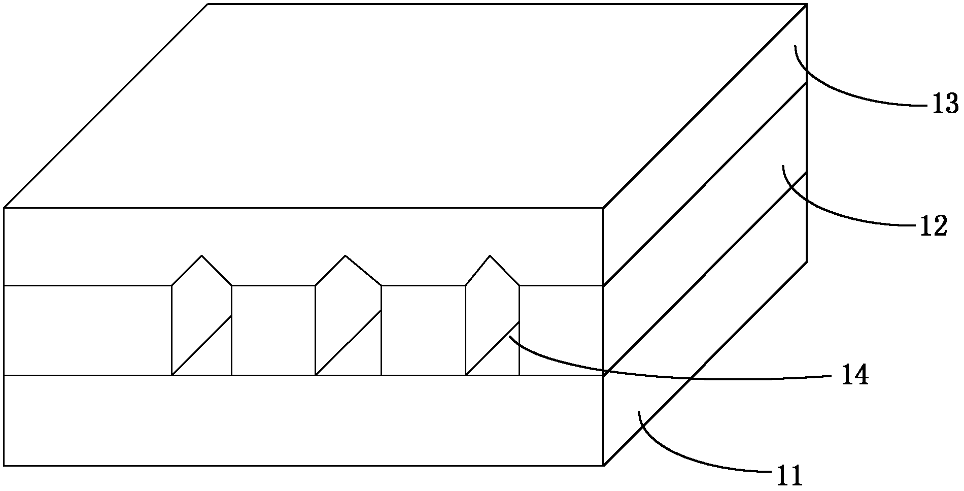
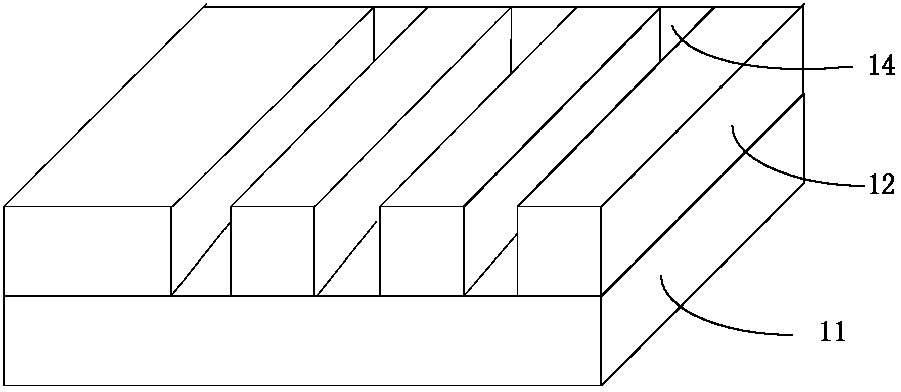
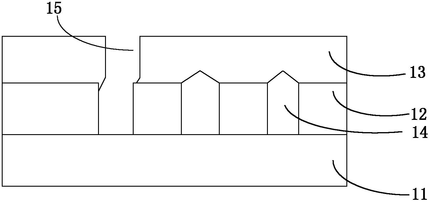
[0041] As mentioned in the background, the air gap in the prior art is in the shape of a long strip groove. When the top dielectric layer is deposited on it, the layer is easy to collapse. The self-alignment accuracy of the holes is required to be high, and the present invention proposes to use photolithography and etching to form air gaps in the intermetallic dielectric layer of the metal interconnection structure; wherein, the air gaps are honeycomb-shaped distributed A fat belly-shaped structure with small top and bottom areas and a large middle area. Compared with the elongated slot-shaped air gaps in the prior art, the honeycomb distribution has a greater impact on the top dielectric layer when depositing the top dielectric layer. The supporting force of the electrical layer is evenly distributed, so that the mechanical strength of the layer is enhanced and it is not easy to collapse. In addition, the area of ​​the top and bottom is smaller than that of the elongated groov...


PUM


Abstract

The invention provides an air gap forming method which includes: firstly, a metal interconnection structure is provided, and the metal interconnection structure comprises metal structures and an intermetallic dielectric layer between the metal structures; photoetching and etching are performed on the intermetallic dielectric layer of the metal interconnection structure to form air gaps; the air gaps are sealed by a deposition interlayer dielectric layer; finally a conductive plug is manufactured on the interlayer dielectric layer; and the air gaps formed in the photoetching and etching step are of a plurality of D-shaped structures which are distributed in the shape of a honeycomb and have small top and bottom areas and a large middle area. The invention further provides the air gap structures and a semiconductor device with the structures. A top dielectric layer formed by the technical scheme is enhanced in mechanical strength, is not prone to collapse, and has low requirements on self-alignment accuracy when through holes are formed in a next process.

Description

technical field [0001] The invention relates to the field of semiconductor manufacturing, in particular to an air gap, a method for forming the air gap and a semiconductor device. Background technique [0002] When the semiconductor industry evolves the process technology below 90nm, the distance between adjacent connecting lines becomes smaller and smaller, and the capacitance generated between them becomes larger and larger. This capacitance is also called parasitic capacitance. This capacitance not only affects the operating speed of the chip , also has a serious impact on the reliability of the devices on the chip. In order to alleviate this problem, the semiconductor process replaces interlayer dielectric layers and intermetal dielectric layers with high dielectric constants such as silicon oxide (k=4.2) with low dielectric materials (3.0<k<4.2) to reduce the adjacent capacitance between the wires. When the process technology evolves to 32-45nm, the problem of c...

Claims


Application Information

Patent Timeline
Patent Type & Authority Applications(China)
IPC IPC(8): H01L21/768H01L23/522
Inventor 符雅丽张海洋
Owner SEMICON MFG INT (SHANGHAI) CORP
Why Eureka
Try Eureka