Liquid crystal panel and manufacturing method thereof

A technology for a liquid crystal panel and a manufacturing method, which is applied in semiconductor/solid-state device manufacturing, instruments, optics, etc., can solve the problems of reduced reliability of liquid crystal panels, aggravated corrosion risks, and aggravated frame light leakage, so as to avoid reliability problems and avoid borders. Light leakage, reducing the effect of border light leakage

Active Publication Date: 2013-07-03
BEIHAI HKC OPTOELECTRONICS TECH CO LTD
View PDF7 Cites 14 Cited by
  • Summary
  • Abstract
  • Description
  • Claims
  • Application Information

AI Technical Summary

Problems solved by technology

[0006] However, on the one hand, the current black matrix is ​​generally made of resin, and the resin material itself has the problem of easy water absorption. Therefore, in the long-term use of the liquid crystal panel, the moisture absorbed by the resin material from the environment will easily cause liquid crystal Corrosion of the metal structure in the panel, so designing the black matrix 12 too long will obviously further aggravate the risk of corrosion, resulting in a decrease in the reliability of the liquid crystal panel
[0007] On the other hand, the shading effect of the current black matrix of resin material is much inferior to that of the black matrix of chrome material in the early stage. The black matrix 12 leaks outside, so simply relying on the black matrix 12 is actually unable to completely prevent the frame from leaking light
Furthermore, when high-brightness backlights become more and more a development trend, the high brightness of backlights will obviously further aggravate the light leakage phenomenon of the frame

Method used


Image

  • Liquid crystal panel and manufacturing method thereof
  • Liquid crystal panel and manufacturing method thereof
  • Liquid crystal panel and manufacturing method thereof

Examples


Embodiment 1

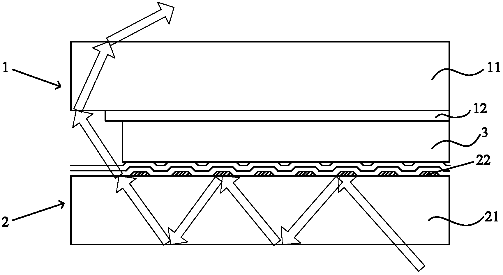
[0040] The liquid crystal panel in this embodiment includes a display area and a frame area surrounding the display area. figure 2 Shown is a schematic cross-sectional view of the frame area of ​​the liquid crystal panel. Such as figure 2 As shown, the liquid crystal panel includes a color filter substrate 1 and an active device array substrate 2 , which are connected by a sealant 3 .

[0041] The color filter substrate 1 includes a base 11 and a black matrix 12 , while other structures of the color filter substrate 1 are not shown in the figure.

[0042] The active device array substrate 2 includes a base 21 , common electrode lines 22 , a transparent dielectric layer 23 and a transparent dielectric layer 24 , and both the transparent dielectric layer 23 and the transparent dielectric layer 24 can be made of, for example, silicon nitride. In the display area, a plurality of thin film transistors (not shown) are arranged on the substrate 21 . Wherein, the common electrode...

Embodiment 2

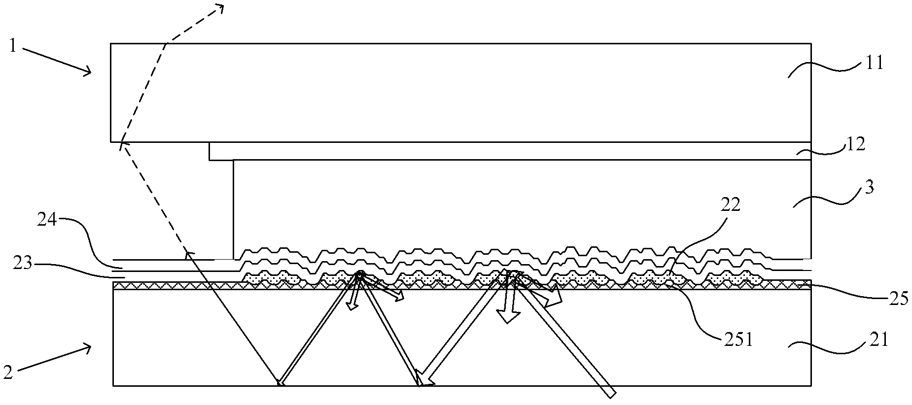
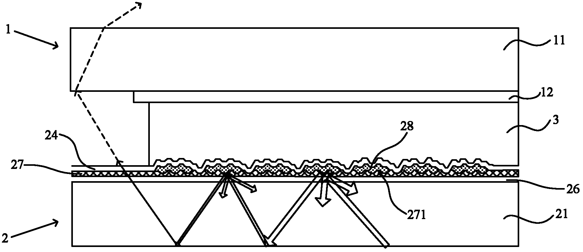
[0048] The liquid crystal panel in this embodiment also includes a display area and a frame area surrounding the display area. image 3 Shown is a schematic cross-sectional view of the frame area of ​​the liquid crystal panel. In this embodiment, the substrate 11, the black matrix 12, the sealant 3, the transparent medium layer 24 and the substrate 21 are all the same as those in Embodiment 1, and in the display area, the substrate 21 There are also a plurality of thin film transistors (not shown in the figure), but the layer structure between the transparent medium layer 24 and the substrate 21 is different from that of the first embodiment.

[0049] In this embodiment, in the frame area, a transparent layer 26 , a light absorbing layer 27 , and common electrode lines 28 are on the substrate 21 in order, and the transparent medium layer 24 is on the common electrode lines 28 . The common electrode line 28 has a first diffuse reflection structure, the first diffuse reflection...


PUM


Abstract

The invention discloses a liquid crystal panel and a manufacturing method thereof. The liquid crystal panel comprises an active element array substrate and a color filtering substrate which are connected with each other through frame sealing glue, wherein the active element array substrate comprises a substrate, a public electrode wire and a plurality of thin film transistors; the color filtering substrate comprises a black matrix; the liquid crystal panel is provided with a display area and a border area surrounding the display area; the active element array substrate further comprises a light absorbing layer having a light absorbing property; the light absorbing layer is positioned in the border area, and is positioned between the substrate and a metal structure which is closest to the substrate in the border area; the metal structure is provided with a first diffused reflection structure; and the first diffused reflection structure is used for making light coming from a backlight source enter the first diffused reflection structure to generate diffused reflection. Due to the adoption of the liquid crystal panel, the border light leakage of the liquid crystal panel can be reduced greatly on the premise of not elongating the black matrix till the edge of the black matrix is aligned with the edge of the substrate.

Description

technical field [0001] The invention relates to a liquid crystal panel and a manufacturing method thereof, in particular to a liquid crystal panel which avoids frame light leakage and a manufacturing method of the liquid crystal panel. Background technique [0002] A liquid crystal display generally includes a liquid crystal panel and a backlight source. The liquid crystal panel usually includes an active element array substrate, a color filter substrate and a liquid crystal layer between the two. [0003] A liquid crystal panel usually has a display area and a frame area surrounding the display area. figure 1 Shown is a schematic cross-sectional view of the frame area on one side of the liquid crystal panel. Such as figure 1 As shown, a color filter substrate 1 includes a base 11, a plurality of color filter units (not shown) disposed on the base 11 and a black matrix 12, the black matrix 12 is actually in the display area and There are distributions in the frame area. T...

Claims


Application Information

Patent Timeline
Patent Type & Authority Applications(China)
IPC IPC(8): G02F1/1335G02F1/1343G02F1/136G02F1/1333H01L21/77
Inventor 梁艳峰张秋林胡文晓
Owner BEIHAI HKC OPTOELECTRONICS TECH CO LTD
Why Eureka
Try Eureka